Cellular Hardware & Electronics
by Kingpin (L0pht Heavy Industries)
The rapid increase of cellular cloning software has led me to write this article on the other side of cellular hacking - hardware and electronics. Hardly anybody recognizes the complexity behind their phones and other devices, and most people just use the technology without understanding how it works. The hardware and electronic aspect of hacking is equally as important as the software-side, and to me is more interesting.
Many older transportable and mobile cellular phones are designed a bit differently inside compared to those built after the mid-1980s. While newer phones store Number Assignment Module (NAM) information inside various types of EEPROMs, older phones store the information a Programmable Read-Only Memory (PROM). A PROM cannot be erased once programmed, and is used for specific one-time-programmable applications.
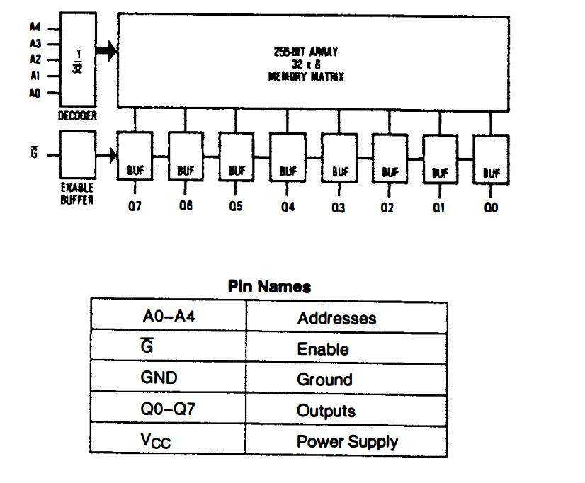
Changing the NAM nowadays is easily done through the phone's keypad, but when these older phones were made, there was no visible need to change any of this information once it was programmed. The most common type of PROM used is 32 words by 8 bits (256 bits total) capacity with tri-state outputs. Each address (word) holds 8-bits. These chip s are fairly simple to read, but not as simple to program. One mistake in programming and you will have to start over with a new chip. Many tiny fuses are inside the chip and in order to program a certain bit into that address, the fuse will either break (blow) or stay intact, thus producing a 1 (blown) or a 0 (intact). The fuses in these chips are made from a special type of metal designed to break with a small a mount of current. Two popular part numbers for this type of PROM are 74S288 and 82S123.
The NAM PROM is easily accessible and almost always held in a Zero-Insertion Force (ZIF) socket. Information stored on this chip is as follows (detailed descriptions can be found in various other texts and articles):
       LU - Local Use Flag
      SCM - Station Class Mark
      GIM - Group ID Mark
       EE - End-to-End Signaling Flag
      REP - Speed Dialing (on/off)
       HA - Horn Alert Flag
       HF - Hand-Free Mode (on/off)
       PS - Preferred System Flag
     MIN1 - Mobile Telephone Number (7-digits)
     MIN2 - Area Code of Mobile Phone Number
     IPCH - Initial Paging Channel
     SIDH - System Identification for the Home System
   ACCOLC - Access Overload Class
 MIN MARK - Send MIN2 (on/off)
LOCK CODE - Lock/Unlock Code
|
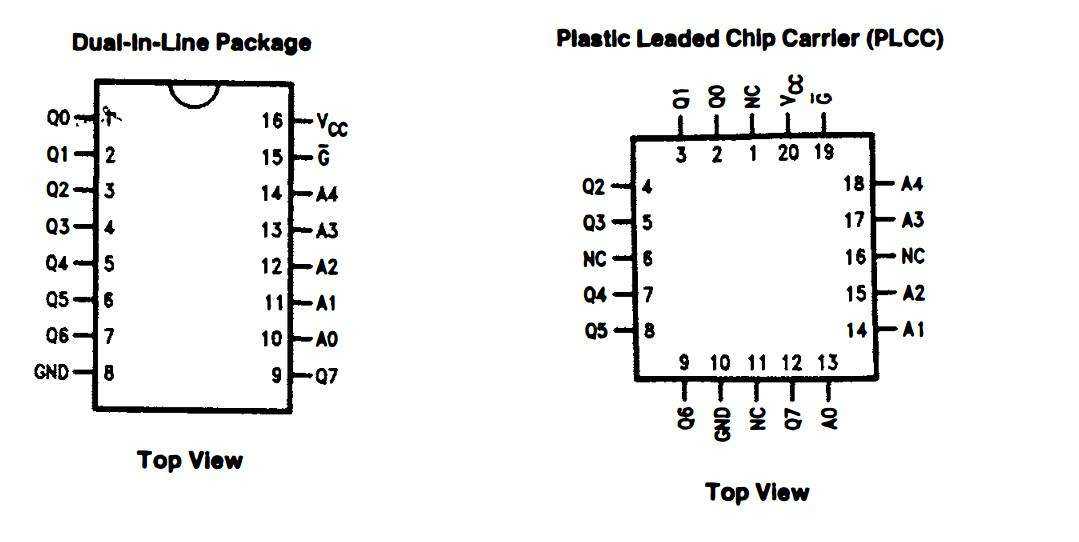
Reading these chips is easily done with a small circuit which took me only 10 minutes to design and build using a CD4040 decade counter and eight LEDs (for the 8-bit output at each address). Pin-outs for the necessary chips are shown at the end of the article. When reading the PROM, use a toggle switch to cycle through each address, writing down a "1" or a "0" for the output of each bit. It seems like a tedious task but it works.
The information in the PROM is stored in a peculiar format general to all of the older model phones. By looking at the 1s and 0s obtained from the PROM and manipulating them in a certain way, you can get whatever NAM data you need. When using the data collected from the PROM, read it in the right-to-left direction. It is stored this way for use by the microprocessor.
I am going to use an example from one of my phones (with MIN1 and MIN2 changed) so it will be easier to see the layout - the sections in bold-type are what you want to pay attention to.
The format for the NAM storage is as follows:
Word Binary Function 00 00000000 00-01 SIDH (15-bits) 01 11100000 02 10000001 MIN MARK (1-bit) + LU (1-bit) 03 11001000 03-04 MIN2 (10-bits) + Home System A/ B (1-bit) + Roam Inhibit (1-bit) 04 00001101 (MIN2 binary = 0100111011) 05 01110000 05-08 MIN1 (24-bits) 06 10101100 (MIN1 binary = 111000110101011001100110) 07 01100110 08 00000110 09 00000000 SCM (4-bits) 0A 10000000 0A-0B - IPCH (11-bits) 0B 10110010 0C 10100000 ACCOLC (4-bits) 0D 10000000 PS (1-bit) 0E 01010000 GIM (4-bit) 0F 00100101 0F-10 LOCK CODE (each digit = 4-bits) 10 00001010 0 in code = A in hex - This code: 045 11 10000001 REP (1-bit) + EE (1-bit) 12 00000001 HF (1-bit) + HA (1-bit) 13 10010000 13-1D empty - except for special [unknown] options 14 00000000 15 00000000 16 00000000 17 00000000 18 00000000 19 00000000 1A 00000000 1B 00000000 1C 00000000 1D 00000000 1E 01001011 NAM Checksum Adjustment 1F 00000001 NAM Checksum |
The last two addresses, 1E and 1F, are used for checksum purposes. The NAM Checksum (1F) is simply the (binary) sum of all the bits in the PROM. It must have a "0" in the last two digits and the NAM Checksum Adjustment (1E) is used to make that so. Add whatever bits you need to the Checksum Adjustment after you have reconfigured your NAM information.
To convert MIN2 and MIN1 from binary to the actual numbers (or vice versa), you will have to do the following:
MIN2 - Convert the binary of MIN2 (10-bits) into standard decimal. Using the table below, add one digit to each decimal number, and you will have the area code.
Coded Digit : 0 1 2 3 4 5 6 7 8 9 Phone Digit : 1 2 3 4 5 6 7 8 9 0 |
MIN1 - First, split up the binary of MIN1 into sections of 10-bits, 4-bits, and 10-bits (there should be 24-bits total in MIN1). Convert the first and last 10-bits like MIN2. As a result, you will have two 3-digit segments. Those are the beginning and the end of the phone number. Convert the middle 4-bits directly into standard decimal, and that will be your middle-digit (do not convert like above).
If you want to change the NAM information often and easily, you could substitute an Erasable Programmable Read-Only Memory (EPROM) in place of the PROM. Since most memory chips are designed to work with one another, using TTL-compatible voltages, this becomes possible. The pin-outs are not the same (the PROMs are usually 16-pin chips and EPROMs range from 24- to 40-pins), but matching the address lines, Vcc, Ground, and outputs should do the trick.
Just convert each 8-bit word from the PROM into its hexadecimal equivalent and program it into the correct address in the EPROM. By using an EPROM instead, it can easily be erased with ultraviolet light and reprogrammed with new data.
Contrary to many old text files which said the Electronic Serial Number (ESN) is stored in the same chip as the NAM information, the ESN is stored in another PROM. After identifying virtually every chip in my phone trying to find where the ESN was stored, I came across another 32-word by 8-bit PROM. It was soldered directly onto a separate PC board. Each phone's ESN PROM I have looked at has had the ESN information stored in a different fashion. Try to identify as many chips as you can by using data books and calling the manufacturers.
Cellular phones have much more potential than free calls. Looking at the hardware, the guts of an electronic device, is the best way to learn first-hand how the technology operates.