| 9600 Baud Packet Radio Modem Design |
| by James Miller, G3RUH |
This placement: ftp.amsat.org /amsat/articles/g3ruh/a109.zip
Date: 1995 Mar 29
First placement: Papers of ARRL 7th Computer Networking Conference (US),
Oct 1988. pps 135-140
Other placements: Proceedings of the first RSGB Data Symposium, Harrow,
England July 1988. (12 pps).
Packet: Speed, More Speed and Applications, ARRL 1995.
ISBN 0-87259-495-5
Corrections: Minor edits and update 1994
Size: 22,000 bytes 3400 words 450 lines
---------------------------------------------------------------------------
9600 Baud Packet Radio Modem Design
-----------------------------------
James Miller BSc, G3RUH
3 Benny's Way
Coton
Cambridge
CB3 7PS
England
ABSTRACT
The theoretical minimum audio bandwidth required to send 9600 baud binary
data is 4800 Hz. Since a typical NBFM radio has an unfiltered response
from zero to some 8 kHz, transmission of 9600 baud binary data is perfectly
possible through it. This paper describes a successful implementation.
INTRODUCTION
The standard packet VHF/UHF radio data rate is 1200 baud because all TNCs
provide an internal modem for this speed, and the two-tone AFSK audio
spectrum suits unmodified voiceband radios comfortably. However all TNCs
can generate much higher data rates, and most FM radios have an unrealised
audio bandwidth of some 7-8 kHz or more. So in many cases 9600 baud radio
transmission is entirely practical with them.
This design is a high performance full duplex modem designed for packet use
with most voiceband NBFM radios, assuming only minor modifications.
A key feature of this modem is its digital generation of the transmit audio
waveform. Precise shaping compensates exactly for the amplitude and phase
response of the receiver. This results in a "matched filter" system, which
means that the received audio offered to the data detector has the optimum
characteristic ("eye") for minimum errors. It also allows very tight
control of the transmit audio bandwidth.
MODEM FEATURES
Here is a summary of the modem features.
* MODULATION: FM. Audio applied direct to TX varactor. +/- 3 kHz
deviation gives RF spectrum 20 kHz wide (-60db). Fits standard channel
easily.
* TX MODULATOR: 8 bit long digital F.I.R. transversal filter in Eprom for
transmit waveform generation (12 bit optional). Gives "brick wall" audio
spectrum. Typically -6 db at 4800 Hz, -60db at 7500 Hz. Allows
compensation for receiver (the channel) to achieve perfect RX "eye". Up to
32 TX waveforms, jumper selectable. Output adjustable 0-8v pk-pk.
* SCRAMBLER (Randomiser): 17 bit maximal length LFSR scrambler, as per
K9NG system, and UoSAT-14/22/23 etc. Jumper selectable Data or BERT (bit
error rate test) mode.
* RX DEMODULATOR: Audio from receiver discriminator, 10mv-10v pk-pk. 3rd
order Butterworth filter, 6 kHz. Data Detect circuit for use on simplex
(CSMA) links. Independent un-scrambler.
* CLOCK RECOVERY: New digital PLL clock recovery circuit with 1/256th bit
resolution. Average lock-in time 50 bits (depends on SNR).
* CONNECTS to AX.25 TNC "Modem Disconnect" jack. Suitable for TNC-2 and
any other provided the internal modem can be bypassed. Standard TNC
digital connections needed: TXData, TXClock (16x bit rate), RXData, Data
Detect DCD, GND. RXClock available. RADIO: TXAudio, RXAudio, GND, All
connections via 0.1" pitch pads for SIL connectors or direct soldering.
Unwired DIN 41612 96-way connector (use optional).
* POWER CONSUMPTION: 10 - 15 v DC at 40ma (CMOS Roms), 170 ma (NMOS Roms).
Total 19 ICs (13 CMOS, 2 DACs, 2 op-amps, 2 Eproms). 5 volt regulator and
heatsink.
* OTHER FEATURES: The only set-up is TXAudio level. Channel calibration
facility. Audio loopback. No hard-to-get parts.
* PCB: 160x100mm (single Eurocard format). Top professional quality,
double sided, maximum copper ground plane, plated through, solder resist,
yellow silk-screen. Four 3.3mm mounting holes.
APPLICATION - TNCS
This modem is obviously only suitable for a TNC if its internal modem can
be bypassed, and if it provides for the TTL digital signals:
* TXData e.g. TNC-2 J4-19
* TXClock (16x data rate) J4-11
* RXData J4-17
* Data Detect ("DCD") J4- 1
* GND J4-15
* RXClock (optional) not used
TAPR TNC-2 based designs do this, typified by the TNC-2, PK-80, MFJ-1270,
TNC-200. Close relatives (but with minor variations) are Tiny-2, Euro
TNC2C, BSX-2, PK-87, PK-88 and TNC-220. The necessary interface is at the
"modem disconnect" jack.
The modem's use is not confined to TNCs, however. Some of the recent
multiport packet switches, indeed any signalling system, is suitable if it
can service the minimum signal set above.
APPLICATION - RADIOS
The ideal would be to have a flat DC-8 kHz radio link. The "better" the
TX and RX specification, the better the received data at the detector, and
hence less susceptibility to errors.
Some apparently horrid receiver responses still offer useable service, but
with a typically 3 db reduction in performance. A good radio achieves
about 1.5 db implementation loss compared with a perfect link.
Remember that one is pushing most radios to their limit since they were
designed for speech where even 100% distortion is still intelligible. A
little more finesse is required for data transmission.
RECEIVERS
* NBFM design
* Output from discriminator (essential)
* Response to DC (virtually essential)
* Response no worse than -4 db at 4.8 kHz
* No worse than -10 db at 7.2 kHz
* As smooth/flat a phase delay as possible
* As smooth an amplitude response as possible
* Little change in response with 2 kHz de-tuning off-channel.
On the whole, most receivers will perform as required. Those with the
least complicated IF filtering appear best, especially those with type "D"
20 kHz channel filters (e.g. CFW455D), though the "E" (16 kHz) is OK too.
Radios with dozens of tuned circuits tend to be fussy, and should be
carefully aligned for even response, decent linearity, phase delay and
mistuning performance.
TRANSMITTERS
* MUST generate true FM
* Response DC to 7.2 kHz (essential).
Transmitters based on Xtal oscillator/multipliers are likely to be the most
appropriate. (Usually base stations. So who wants to tie up a multimode
radio on a link anyway!)
Transceivers (synthesised or not) that have quite separate oscillator sub-
systems for generating FM and possibly SSB/CW, which is then mixed with a
synthesised source to produce the final carrier are OK.
Simpler synthesised FM transmitters, where the varactor modulated
oscillator is within the synthesis PLL are generally not useable, as the
PLL tracks the modulation, and so you get no LF response, There are ways
around this by modulating the reference xtal, called two-point modulation.
Remember you need true FM, which preferably means a varactor pulling the
oscillator frequency, NOT phase modulating a tuned circuit.
9600 BAUD MODEM - DESCRIPTION
All the bits and pieces required to interface digital data to a radio are
called a "modem", short for modulator/demodulator. These two functions are
complementary, and essentially separate even though there may be shared
parts such as clocks and power supplies etc. Figure 1a-1d is the full
circuit diagram of production boards, issue 3. Issue 1 were prototypes,
issue 2 the beta-test models.
TRANSMIT RANDOMISER/SCRAMBLER
Data for transmission is first passed through a randomiser or scrambler.
This ensures that there are no long runs of all "1"s or "0"s or repeated
patterns. There are several good reasons for doing this [2].
One is that the channel is not DC coupled. It could never be so in an FM
system unless one could guarantee both transmitter and receiver were always
exactly on frequency and had no drift. As this is virtually impossible to
achieve, one simply AC couples the channel, i.e. gives it a response down
to a few Hz, and exploits the feature of the randomised data that it has a
negligible DC component.
Secondly, since the data stream is now randomised, its spectral energy is
evenly spread out at all times. Intense spectral lines do not suddenly
appear and create sporadic splatter into nearby channels.
A third reason is that since the data is guaranteed to have a regular
supply of ones and zeros, the receiver's bit clock recovery and
demodulation circuits work better.
Not surprisingly a burst of data sounds like a burst of radio noise, and is
quite hard to distinguish from the unsquelched background.
TRANSMIT WAVEFORM GENERATOR
The transmit waveshape(s) are stored in an EPROM. An 8 bit shift register
contains the most recent bits, which are used to look up profile for the
middle one. Four samples/bit go to make up the profile. In this way the
transmitted waveform is synthesised not only from the present bit's state,
but also four that preceded it and four to come.
The 8 bit value output from the EPROM is converted to a voltage by an
inexpensive single-rail DAC, and is then analogue low pass filtered to
remove harmonics of the clock and associated discrete phenomena. This is
variously called "anti-aliasing" or "smoothing" or "interpolating". Either
way, it simply joins up the dots!
The arrangement as a whole is a "finite impulse response filter", or FIR
for short.
The Transmit EPROM is normally a type 27C128 and can hold between sixteen 8-
bit long FIRs, to one 12-bit long FIR or various combinations. A 27C256
can also be used offering up to 32 responses. NMOS roms are also suitable.
MODEM RECEIVE - FILTER/DETECTOR
Audio from the receiver discriminator is passed through a gentle input
filter which removes out of band spurious noise, particularly IF residue.
The signal is then limited and detected by sampling at the correct instant.
UNSCRAMBLER
The detected data, still randomised is then passed through an
unscrambler, where the original data is recovered, and this goes off to the
TNC. A scrambler is very simple, consisting of a 17 bit shift register and
3 Exor gates. See for example fig 3 of [2].
The scrambling "polynomial" is 1 + X^12 + X^17. This means the currently
transmitted bit is the EXOR of the current data bit, plus the bits that
were transmitted 12 and 17 bits earlier. Likewise the unscrambling
operation simply EXORs the bit received now with those sent 12 and 17 bits
earlier. The unscrambler perforce requires 17 bits to synchronise.
This polynomial was deliberately chosen to be the same as implemented by
Goode [1] in an earlier modem design. It will also be used on one of the
UoSAT-C satellite downlinks.
B.E.R.T. TESTING
A particularly useful by-product of scramblers is "bit error rate
testing" or BERT for short. Suppose the transmitted data is held to all
"1"s. Then a receiver's error-free output should also be all "1"s even
though the transmitted data is quite random. So to test the quality of a
link one merely sends all "1"s and attaches a counter at the other end.
If one bit is corrupted due to channel noise, the error will in fact appear
exactly 3 times at the receiver output, because there are 3 versions of the
scrambled stream exored together. Even though one error creates two more,
this doesn't matter because just the single error is enough for a packet to
be rejected.
Incidentally, randomisers/scramblers don't really violate rules concerning
codes and ciphers any more than do ASCII, Baudot or Morse. Since the
scrambling algorithm is freely published, the meaning of the data is not
obscured.
RECEIVE CLOCK RECOVERY
The demodulator must extract a clock from the received audio stream.
It's needed to time the receiver functions, including the all-important
data detector.
The familiar TAPR TNC-2 state machine is not satisfactory in this
application, as its resolution is only 1/16th bit. It can show jitter up
to +/- 5/16ths of a bit in this narrow band application, which gives bad
performance for detector timing.
This modem uses a new digital phase locked loop (DPLL) with a resolution of
1/256th bit.
The received audio is limited, and a zero crossing detector circuit
generates one cycle of 9600 Hz for each zero-crossing (a proto-clock).
This is compared with a locally generated clock in a phase detector based
on an up/down counter. The counter increments if one clock is early,
decrements otherwise. This count then addresses an Eprom in which 256
potential clock waveforms are stored, each differing in phase by 360/256
degrees. In this way the local clock slips rapidly into phase with that of
the incoming data.
RX Clock lock-in time depends on the signal to noise ratio, and the initial
phase error. A signal that's already in phase pulls into lock within 0
bits. A noise-free signal exactly out of phase will pull in to a point
where data errors cease in about 80 bits. A very noisy signal could take
up to 200 bits. In practice, an average figure is around 50 bits, or about
5 ms at 9600 baud.
Proto-clock and local clock are also compared in an exor gate, and when
they are "in-phase", a Data Carrier Detected signal (DCD) is sent to the
TNC. High or low options are available.
TRANSMIT WAVESHAPE SYNTHESIS
As mentioned, a strength of this modem is its digital generation of the
transmit audio waveform. The precise shaping compensates exactly for the
amplitude and phase response of the receiver. It also allows very tight
control of the transmit audio bandwidth.
The waveform is synthesised as follows. First the "ideal" receiver output
waveform (at the "eye point") is defined. This waveform, for one isolated
bit, has a perfect "eye". It has a value of +1 at T=0 and a value of 0 at
+/-T, +/-2T etc where T is a bit period. Its spectrum is flat to 3300 Hz, -
6db down at 4800 Hz, and is absolutely band limited to 6300 Hz. The
waveform is called a "Nyquist Pulse".
Next the channel frequency and phase response is measured. It is made up
of several contributions; the modem transmit anti-alias filter, the radio
transmitter response, the receiver response and finally the modem receive
filter. In practice most of these components are already characterised, so
it's only necessary to characterise the receiver part explicitly.
Now the ideal Nyquist pulse's frequency response is divided by the channel
frequency response to give the ideal transmit spectrum. This is then
Fourier transformed to the time domain, and specifies EXACTLY the waveform
of a transmitted bit that would pass right through the system to emerge
with the desired Nyquist shape.
This desired waveform will have a time span of some 15 bits or more
duration. However only the middle 8-12 bits duration will have any
significant amplitude. So the extremes are gracefully smoothed off to
exactly 8 bits span, a process known as windowing.
As a verification check, the new pulse is now "sent" mathematically
forwards through the channel to assay the effect of having had to truncate
it, and the "eye" point vertical jitter calculated. It is typically +/-
10% of a unit bit amplitude.
This calculation only defines a waveshape for one isolated bit. But it
will extend over 8 bits elapsed time. So the final stage in the synthesis
is to add up the impulse responses of all possible 256 combinations of
preceding and trailing bits to give the true "convolved" waveform that is
finally used. The waveform is then stored as numbers in an Eprom.
The software to do the equalisation is programmed in BASIC, except for the
Fourier transforms (512 point complex FFTs) which are machine coded for
speed. The waveforms and spectra are displayed graphically at every
stage. Figures 2 a-f illustrate equalisation of a fairly extreme specimen
of radio, a Midland 13-509 220 MHz transceiver (USA).
PERFORMANCE
Users accustomed to the speed of a typical 1200 baud channel are usually
astonished to see 9600 baud data scrolling off the screen at full speed.
In the perfect environment of audio loopback, the error performance of the
modem has been measured, and the implementation loss is about 1 db. In
other words the modem itself does not introduce significant degradation in
system performance.
On the other hand it is not very appropriate to describe the modem in terms
of microvolts at an FM receiver input. So much depends on the particular
specimen, the environmental noise level, frequency drift, and goodness of
equalisation. Steve Goode [1] has given detailed results for one typical
situation, and it should be clear from this that there can be no simple
snap performance measure, other than "does it work".
What can be said is that once the received signal strength puts the
receiver output above the "spitching" threshold, and into smooth noise,
(and that's only a 1db spread in RF level!) the 9600 baud system becomes
essentially error free. So a radio link needs to be just over the noise
threshold for good performance - as also does 1200 baud AFSK.
Remember, the purpose of this modem is to provide a reliable high speed
communications facility, not to scrape weak DX off the noise floor!
EPROM SERVICE
The standard transmit Eprom contains waveforms for 16 named receivers.
One of these (usually selection no. 10) is almost certain to be
satisfactory for an arbitrary receiver. If not, the author offers a
customising service. Full details are included in the modem Instruction
Booklet. New receivers will gradually be added to the standard Eprom as
users supply more data.
PCB AVAILABILITY AND SUPPORT
This project is supported with a Printed Circuit Board and full
instructions. At the time of writing (88 Aug 16) some 200 are in worldwide
use. (Update 1994 Nov: about 15,000).
ORDERING
PCB #18 post paid UK/Europe, #19 air-mail elsewhere. CMOS TX and RX
Eproms (programmed), when ordered at the same time as the PCB, #6/pair.
DACs #5/pair. Built and tested PCB #65. Any eproms ordered separately #5
each chip. You are free to copy the eproms if you wish.
Sterling Cheques, Eurocheques (max #150), Travellers Cheques, Cash, or bank
draft drawn on a London bank. Also electronic funds transfer, please add
#6 bank charges. No credit cards. You can "buy" English pound notes at
many banks. I will also accept US dollars in cash only (green notes/
travellers cheques) at a rate of $2 per pound. In case of difficulty,
contact me. Prices include postage and packing.
Note: # = GBP = Pounds Sterling.
James Miller G3RUH, 3 Benny's Way, Coton, Cambridge, CB3 7PS, England
Tel: +44 1954 210388 Fax: +44 1954 211256
COMMERCIAL AVAILABILITY
The modem design is also incorporated in products from:
PacComm Inc: NB-96
Kantronics: DE-9600
MFJ: MFJ-9600
Tasco: TMB-965
Symek: TNC2-H
and about a dozen more licensees.
ACKNOWLEDGMENTS
Scores of people provided feedback and support for this project. These
include some 20-25 beta testers world wide who provided many responses for
the eproms, design criticism and debugged all those wretched non-standard
"standard" modem disconnect headers! Gwyn Reedy W1BEL of PacCom Inc and
Phil Bridges G6DLJ of Siskin electronics Ltd have been instrumental in
promoting the design at both amateur and commercial levels. I also
acknowledge the pioneering work of Steve Goode [1] who did a lot of spade
work some years ago, and which convinced me all along that this project was
on sound ground. Thanks too to Bob McGwier N4HY for insisting this design
should see the light of day, and not remain the secret weapon of EastNet-
UK's links.
REFERENCES
----------
1. GOODE S. "Modifying The Hamtronics FM-5 for 9600 bps Packet Operation",
Proceedings of the Fourth ARRL Amateur Radio Computer Networking
Conference, pps 45-51.
2. HEATHERINGTON D.A. "A 56 Kilobaud RF Modem", Proceedings of the Sixth
ARRL Amateur Radio Computer Networking Conference, pps 65-75.
CAPTIONS
--------
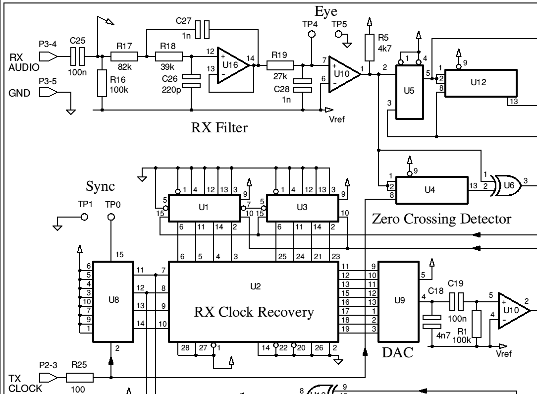

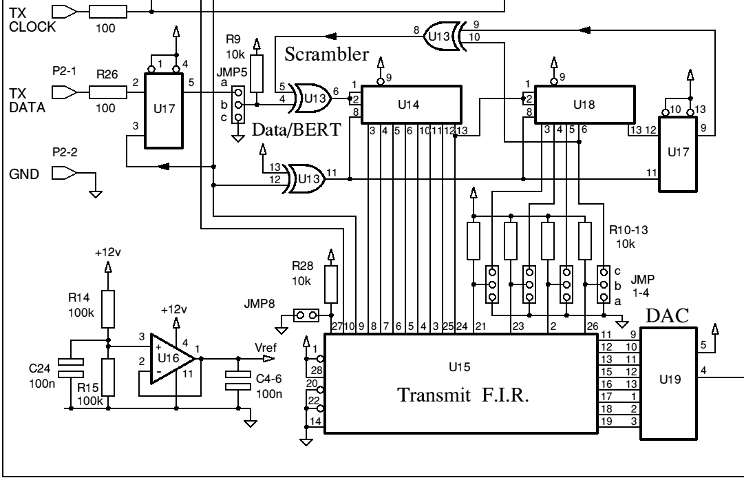
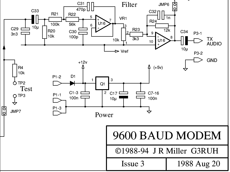
Fig. 1a-d. Modem schematic ; split into 4 parts for legibility.
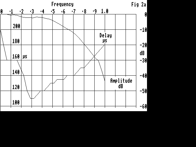 Fig 2a. Frequency response and phase delay of a typical NBFM receiver.
Note that the frequency axis is normalised. f=1.0 corresponds to 9600 Hz.
Fig 2a. Frequency response and phase delay of a typical NBFM receiver.
Note that the frequency axis is normalised. f=1.0 corresponds to 9600 Hz.
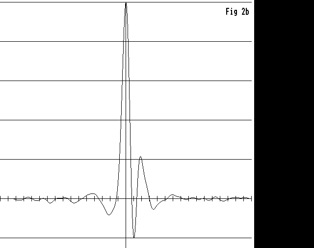 Fig 2b. Impulse response corresponding to fig 2a. Horizontal axis time
"ticks" are at intervals of 1 bit (1/9600 sec), and has been shifted some
125 us so as to centre the peak. An isolated, unequalised bit would emerge
from the receiver shaped like this. A stream of bits would be the sum of
many of these. Bad features such as significant non-zero values at T = -2,
+1 and +2 bits would give rise to substantial inter-bit interference and a
very poor eye, making error free communication impossible. The purpose of
equalisation is to eliminate this phenomenon.
Fig 2b. Impulse response corresponding to fig 2a. Horizontal axis time
"ticks" are at intervals of 1 bit (1/9600 sec), and has been shifted some
125 us so as to centre the peak. An isolated, unequalised bit would emerge
from the receiver shaped like this. A stream of bits would be the sum of
many of these. Bad features such as significant non-zero values at T = -2,
+1 and +2 bits would give rise to substantial inter-bit interference and a
very poor eye, making error free communication impossible. The purpose of
equalisation is to eliminate this phenomenon.
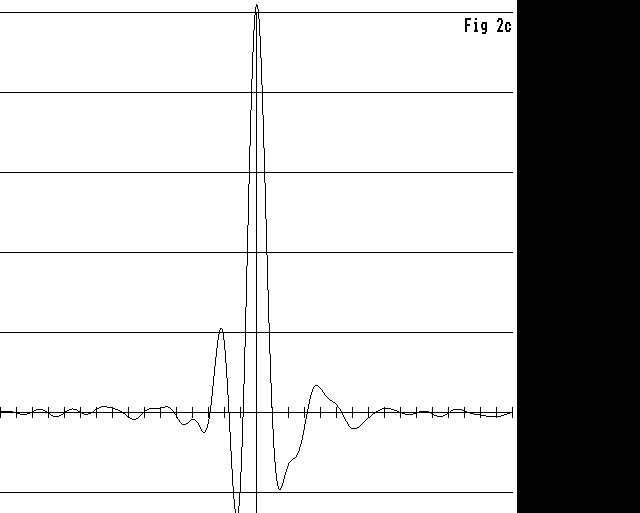 Fig 2c. Equalised Transmit bit. If the transmitter sends an isolated bit
shaped like this, the receiver will give an output like fig 2e. This is
the transmit waveform for one isolated bit. If this corresponds to a
binary "1", a binary "0" is a negative pulse like this.
Fig 2c. Equalised Transmit bit. If the transmitter sends an isolated bit
shaped like this, the receiver will give an output like fig 2e. This is
the transmit waveform for one isolated bit. If this corresponds to a
binary "1", a binary "0" is a negative pulse like this.
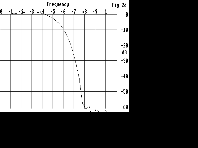 Fig 2d. Spectrum of the transmitted audio pulse of fig 2c.
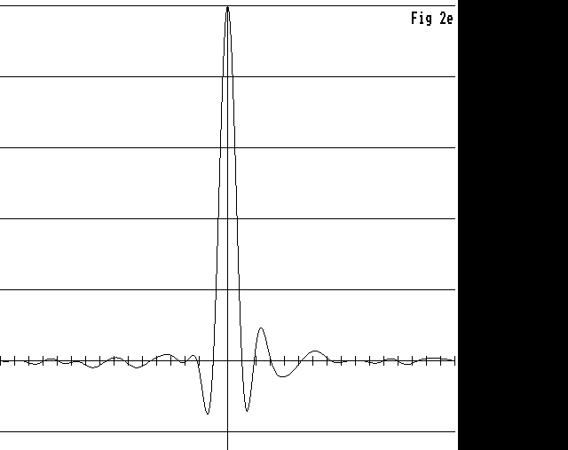 Fig 2e. Receiver output response to an isolated bit which has been
properly equalised. Note that generally zero crossings at the bit ticks
(excepting T=0) are zero. This is the "Nyquist Pulse". In fact the
equalisation is not perfect (e.g. at T=4). This is due to the fairly
extreme radio response chosen for illustrative purposes.
Fig 2e. Receiver output response to an isolated bit which has been
properly equalised. Note that generally zero crossings at the bit ticks
(excepting T=0) are zero. This is the "Nyquist Pulse". In fact the
equalisation is not perfect (e.g. at T=4). This is due to the fairly
extreme radio response chosen for illustrative purposes.
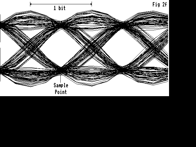 Fig 2f. The convolution of many bits of fig 2e superimposed looks like
this, an "EYE" diagram showing a few hundred bits over 3 bit periods. You
would see this on an oscilloscope. The data detector samples this waveform
at the widest part of the eye. See how as a result of equalisation the eye
is wide open, giving maximum noise immunity. Vertical spread at the sample
point is mainly due to the aberration at T = 4 in fig 2e. Note also the
considerable spread in zero crossing instants typical of narrow bandwidth
systems, which lead to the need for careful clock recovery circuit design.
(C)1988 James Miller G3RUH E-mail: g3ruh@amsat.org
Fig 2f. The convolution of many bits of fig 2e superimposed looks like
this, an "EYE" diagram showing a few hundred bits over 3 bit periods. You
would see this on an oscilloscope. The data detector samples this waveform
at the widest part of the eye. See how as a result of equalisation the eye
is wide open, giving maximum noise immunity. Vertical spread at the sample
point is mainly due to the aberration at T = 4 in fig 2e. Note also the
considerable spread in zero crossing instants typical of narrow bandwidth
systems, which lead to the need for careful clock recovery circuit design.
(C)1988 James Miller G3RUH E-mail: g3ruh@amsat.org
G3RUH 9600 Baud Packet Radio Modem PCB
--------------------------------------
SECTION 7 - COMPONENTS LIST From G3RUH PCB Manual (18 pages)
(See Section 12. for 19200 baud changes)
RESISTORS - (All 2%, 0.4" pitch)
R1,6,14-16,21 100k (6) R8 47k R22 56k
R2,5 4k7 (2) R17 82k R23 3k3
R3 18k R18 39k R24 12k
R4,9-13,20,27-28 10k (9) R19 27k R25,26 100 (2)
R7 33k Note: 4k7 = 4700 ohms, etc
VR1 10k Cermet Trimmer e.g. Spectrol 63, 64 series,
Bourns 3386, 3266, 3296 etc. PCB Drilled for all types.
CAPACITORS
C1-16,19,21-22,24-25 100n 20% monolithic (21) 0.1" pitch (NOT 0.2")
C17,33-34 10u 16v tantalum (3) 0.2" pitch
C18 4n7 20% monolithic ceramic 0.1" pitch
C20 100p 20% monolithic ceramic 0.1" pitch
C23 1n 20% monolithic ceramic 0.1" pitch
C26 220p 2.5% polystyrene Note:
C27-28,32 1n 2.5% polystyrene (3) 100n = 0.1u
C29 3n3 2.5% polystyrene 10n = 0.01u
C30 100p 2.5% polystyrene 4n7 = 0.0047u
C31 470p 2.5% polystyrene 1n = 0.001u etc
INTEGRATED CIRCUITS
U1,3 4029 (2) Up/down counter
U2 27C64 Eprom - RX (or 27C128 and/or NMOS)
U4,7,12,14,18 74HC164 (5) 8-bit shift register
U5,17 74HC74 (2) Dual D type
U6,13 74HC86 (2) Quad EXOR
U8 74HC161 4-bit counter
U9,19 ZN429E-8 (2) DAC (or ZN426E-8), Ferranti or GEC Plessey
U10 LM339N Quad comparator
U11 74HC14 Hex Schmitt inverter
U15 27C128 Eprom - TX (or 27C256 and/or NMOS)
U16 TL084CN Quad op-amp
MISCELLANEOUS
TP0-8 Test points (9)
JMP1-5 3-pin header, male, SIL, 0.1" pitch
JMP6-8 2-pin header, male, SIL, 0.1" pitch
8 x Shorting jacks - 0.1" for JMP1-8
P1 3 pin connector, male, SIL, 0.1" pitch )
P2 6 pin connector, male, SIL, 0.1" pitch ) e.g. Molex etc
P3 5 pin connector, male, SIL, 0.1" pitch )
D1 1N4001 diode (or equivalent 1 amp)
Q1 LM340T5, LM7805CT etc 5v TO-220 voltage regulator
1 x Redpoint TV46 (TO-126 size) Heatsink. 27 degC/w, 22x19 mm
1 x M3x6 screw and nut
IC sockets: 2 x 28-pin. (Optional 14 x 14-pin, 3 x 16-pin). Turned-pin type
recommended.
1 x PCB. Notes: Board is single Eurocard size, 160 x 100mm. Double sided,
plated through, max copper ground-plane, solder resist and legend. Drilled
for an optional DIN 41612 96 way connector. Four 3.3 mm mounting holes
provided on 6.05 x 3.50 inch centres. Two spare 16 pin IC positions.
A suitable heatsink can also be fabricated from a piece of 1.6mm aluminium,
19mm wide x 40 mm, folded into a "U" shape 19x20 and 10mm high sides, and a 3.
3mm hole drilled in the centre.
ORDERING
PCB #18 post paid UK/Europe, #19 air-mail elsewhere. CMOS TX and RX Eproms
(programmed), when ordered at the same time as the PCB, #6/pair. DACs
#5/pair. Built and tested PCB #65. Any eproms ordered separately #5 each
chip. You are free to copy the eproms if you wish.
PAYMENT
Sterling Cheques, Eurocheques (max #150), Travellers Cheques, Cash, or bank
draft drawn on a London bank. Also electronic funds transfer, please add
#6 bank charges. No credit cards. You can "buy" English pound notes at
many banks. I will also accept US dollars in cash only (green notes/
travellers cheques) at a rate of $2 per pound. In case of difficulty,
contact me. Prices include postage and packing.
Note: # = GBP = Pounds Sterling.
James Miller G3RUH, 3 Benny's Way, Coton, Cambridge, CB3 7PS, England
Tel: +44 1954 210388 Fax: +44 1954 211256 g3ruh@amsat.org
COMMERCIAL AVAILABILITY
The modem design is also incorporated in products from:
PacComm Inc: NB-96
Kantronics: DE-9600
MFJ: MFJ-9600
Tasco: TMB-965
Symek: TNC2-H
and about a dozen more licensees.
Higher Speeds with the G3RUH 9600 baud Packet Radio Modem
---------------------------------------------------------
by James Miller G3RUH
1993 Aug 23
The modem is capable of speeds up to 64000 baud. This limit is set by the
maximum rate that the DAC chips can operate. This note describes how to
achieve rates from 4800 to 64000 baud. The slowest speed is suitable for
12.5 kHz channelised radios. The highest speed suits radios that have
broadcast FM bandwidth filters.
To implement a higher speed you need to:
1. Increase your TXData rate (!)
2. Increase the associated TXClock
3. Change some analogue filter components proportional to
the speed increase.
It is not necessary to change either of the eproms. If you are going
for a higher speed, it is likely that the radios involved are "specials"
and you will already have wide bandwidth and flattish group delay, so the
loopback selection 0 from the standard ROM will be OK.
The table below suggests the best conditions for different speeds.
Component references are for my own PCB card. Clones are different.
Data Rate - Baud
Comp 4800 9600 19200 38400 64000
--------------------------------------------------------
R6 220k 100k 47k 22k 15k
R16 100k 100k 100k 47k 15k
R17 82k 82k 82k 39k 12k
R18 39k 39k 39k 18k 5k6
R19 27k 27k 27k 15k 3k9
R21 100k 100k 100k 47k 15k
R22 56k 56k 56k 27k 8k2
C18 4n7 4n7 4n7 1n 680p
C20 220p 100p 47p 22p 12p
C26 ( 470p 220p 100p 100p 220p )
C27 ( 2n2 1n 470p 470p 1n )
C28 ( 2n2 1n 470p 470p 1n )
C29 ( 6n8 3n3 1n5 470p 470p ) 2% or
C30 ( 220p 100p 47p 47p 100p ) better
C31 ( 1n 470p 220p 220p 470p )
C32 ( 2n2 1n 470p 220p 150p )
----------------------------------------------------------
Deviation +/- 1.5 3 6 12 20 kHz ) In FM
IF Bandwidth 8 15 30 60 100 kHz ) Service
----------------------------------------------------------
These modifications have been tested in both amateur and commercial
service. All comments gratefully received, and added to the database.
73 de James G3RUH @ GB7DDX.#22.GBR.EU 1993 Aug 23 [Mon] 0917 utc