Hello Again Professor Hyde,We are currently working on ways to publish this text in a form other than HTML (e.g., Postscript, PDF, Frameviewer, hard copy, etc.). This, however, is a low-priority project. Please do not contact Randall Hyde concerning this effort. When something happens, an announcement will appear on "Randall Hyde's Assembly Language Page." Please visit this WEB site at http://webster.ucr.edu for the latest scoop.
Dallas gave me permission to take orders for the Computer Science 13 Manuals. We would need to take charge card orders. The only cards we take are: Master Card, Visa, and Discover. They would need to send the name, numbers, expiration date, type of card, and authorization to charge $95.00 for the manual and shipping, also we should have their phone number in case the company has any trouble delivery. They can use my e-mail address for the orders and I will process them as soon as possible. I would assume that two weeks would be sufficient for printing, packages and delivery time.
I am open to suggestions if you can think of any to make this as easy as possible.
Thank You for your business,
Kathy Chapman, Assistant
Printing and Reprographics
University of California
Riverside
(909) 787-4443/4444
| Port | Physical Base Address (in hex) | BIOS variable Containing Physical Address |
|---|---|---|
| COM1: | 3F8 | 40:0 |
| COM2: | 2F8 | 40:2 |
| I/O Address (hex) | Description |
|---|---|
| 3F8/2F8 | Receive/Transmit data register. Also the L.O. byte of the Baud Rate Divisor Latch register. |
| 3F9/2F9 | Interrupt Enable Register. Also the H.O. byte of the Baud Rate Divisor Register. |
| 3FA/2FA | Interrupt Identification Register (read only). |
| 3FB/2FB | Line Control Register. |
| 3FC/2FC | Modem Control Register. |
| 3FD/2FD | Line Status Register (read only). |
| 3FE/2FE | Modem Status Register (read only). |
| 3FF/2FF | Shadow Receive Register (read only, not available on original PCs). |
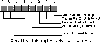
The interrupt enable register I/O location is also common with the Baud
Rate Divisor Register. Please see the next section and "The
Line Control Register" on page 1227 for more information on the
dual use of this I/O location.
| Bits Per Second | 3F9/3F9 Value | 3F8/2F8 Value |
|---|---|---|
| 110 | 4 | 17h |
| 300 | 1 | 80h |
| 600 | 0 | C0h |
| 1200 | 0 | 60h |
| 1800 | 0 | 40h |
| 2400 | 0 | 30h |
| 3600 | 0 | 20h |
| 4800 | 0 | 18h |
| 9600 | 0 | 0Ch |
| 19.2K | 0 | 6 |
| 38.4K | 0 | 3 |
| 56K | 0 | 1 |
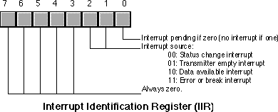
Since the IIR can only report one interrupt at a time, and it is certainly
possible to have two or more pending interrupts, the 8250 SCC prioritizes
the interrupts. Interrupt source 00 (status change) has the lowest priority
and interrupt source 11 (error or break) has the highest priority; i.e.,
the interrupt source number provides the priority (with three being the
highest priority).
The following table describes the interrupt sources and how you "clear"
the interrupt value in the IIR. If two interrupts are pending and you service
the higher priority request, the 8250 SCC replaces the value in the IIR
with the identification of the next highest priority interrupt source.
| Priority | ID Value | Interrupt | Caused By | Reset By |
|---|---|---|---|---|
| Highest | 11b | Error or Break | Overrun error, parity error, framing error, or break interrupt. | Reading the Line Status Register. |
| Next to highest | 10b | Data available | Data arriving from an external source in the Receive Register. | Reading the Receive Register. |
| Next to lowest | 01b | Transmitter empty | The transmitter finishes sending data and is ready to accept additional data. | Reading the IIR (with an interrupt ID of 01b) or writing to the Data Register. |
| Lowest | 00b | Modem Status | Change in clear to send, data set ready, ring indicator, or received line signal detect signals. | Reading the modem status register. |
                 .
                 .
                 .
                in      al, dx          ;Read IIR.
                mov     bl, al
                mov     bh, 0
                jmp     HandlerTbl[bx]
HandlerTbl      word    RLSHandler, RDHandler, TEHandler, MSHandler
When an interrupt occurs, bit zero of the IIR will be zero. The next two
bits contain the interrupt source number and the H.O. five bits are all
zero. This lets us use the IIR value as the index into a table of pointers
to the appropriate handler routines, as the above code demonstrates.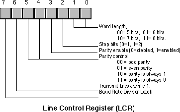
The 8250 SCC can transmit serial data as groups of five, six, seven,
or eight bits. Most modern serial communication systems use seven or eight
bits for transmission (you only need seven bits to transmit ASCII, eight
bits to transmit binary data). By default, most applications transmit data
using eight data bits. Of course, you always read eight bits from the receive
register; the 8250 SCC pads all H.O. bits with zero if you are receiving
less than eight bits. Note that if you are only transmitting ASCII characters,
the serial communications will run about 10% faster with seven bit transmission
rather than with eight bit transmission. This is an important thing to keep
in mind if you control both ends of the serial cable. On the other hand,
you will usually be connecting to some device that has a fixed word length,
so you will have to program the SCC specifically to match that device.
A serial data transmission consists of a start bit, five to eight data bits,
and one or two stop bits. The start bit is a special signal that informs
the SCC (or other device) that data is arriving on the serial line. The
stop bits are, essentially, the absence of a start bit to provide a small
amount of time between the arrival of consecutive characters on the serial
line. By selecting two stop bits, you insert some additional time between
the transmission of each character. Some older devices may require this
additional time or they will get confused. However, almost all modern serial
devices are perfectly happy with a single stop bit. Therefore, you should
usually program the chip with only one stop bit. Adding a second stop bit
increases transmission time by about 10%.
The parity bits let you enable or disable parity and choose the type of
parity. Parity is an error detection scheme. When you enable parity, the
SCC adds an extra bit (the parity bit) to the transmission. If you select
odd parity, the parity bit contains a zero or one so that the L.O. bit of
the sum of the data and parity bits is one. If you select even parity, the
SCC produces a parity bit such that the L.O. bit of the sum of the parity
and data bits is zero. The "stuck parity" values (10b and 11b)
always produce a parity bit of zero or one. The main purpose of the parity
bit is to detect a possible transmission error. If you have a long, noisy,
or otherwise bad serial communications channel, it is possible to lose information
during transmission. When this happens, it is unlikely that the sum of the
bits will match the parity value. The receiving site can detect this "parity
error" and report the error in transmission.
You can also use the stuck parity values (10b and 11b) to strip the eighth
bit and always replace it with a zero or one during transmission. For example,
when transmitting eight bit PC/ASCII characters to a different computer
system it is possible that the PC's extended character set (those characters
whose code is 128 or greater) does not map to the same character on the
destination machine. Indeed, sending such characters may create problems
on that machine. By setting the word size to seven bits and the parity to
enabled and stuck at zero, you can automatically strip out all H.O. bits
during transmission, replacing them with zero. Of course, if any extended
characters come along, the SCC will map them to possibly unrelated ASCII
characters, but this is a useful trick, on occasion.
The break bit transmits a break signal to the remote system as long as there
is a one programmed in this bit position. You should not leave break enabled
while trying to transmit data. The break signal comes from the teletype
days. A break is similar to ctrl-C or ctrl-break on the PC's keyboard. It
is supposed to interrupt a program running on a remote system. Note that
the SCC can detect an incoming break signal and generate an appropriate
interrupt, but this break signal is coming from the remote system, it is
not (directly) connected to the outgoing break signal the LCR controls.
Bit seven of the LCR is the Baud Rate Divisor Register latch bit. When this
bit contains a one, locations 3F8h/2F8h and 3F9h/2F9h become the Baud Rate
Divisor Register. When this bit contains a zero, those I/O locations correspond
to the Data Registers and the Interrupt Enable Registers. You should always
program this bit with a zero except while initializing the speed of the
SCC.
The LCR is a read/write register. Reading the LCR returns the last value
written to it.
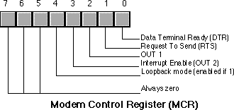
The 8250 routes the DTR and RTS bits directly to the DTR and RTS lines
on the 8250 chip. When these bits are one, the corresponding outputs are
active[5]. These lines are two separate handshake
lines for RS-232 communications.
The DTR signal is comparable to a busy signal. When a site's DTR line is
inactive, the other site is not supposed to transmit data to it. The DTR
line is a manual handshake line. It appears as the Data Set Ready (DSR)
line on the other side of the serial cable. The other device must explicitly
check its DSR line to see if it can transmit data. The DTR/DSR scheme is
mainly intended for handshaking between computers and modems.
The RTS line provides a second form of handshake. It's corresponding input
signal is CTS (Clear To Send). The RTS/CTS handshake protocol is mainly
intended for directly connected devices like computers and printers. You
may ask "why are there two separate, but orthogonal handshake protocols?"
The reason is because RS-232C has developed over the last 100 years (from
the days of the first telegraphs) and is the result of combining several
different schemes over the years.
Out1 is a general purpose output on the SCC that has very little use on
the IBM PC. Some adapter boards connect this signal, other leave it disconnected.
In general, this bit has no function on PCs.
The Interrupt Enable bit is a PC-specific item. This is normally a general
purpose output (OUT 2) on the 8250 SCC. However, IBM's designers connected
this output to an external gate to enable or disable all interrupts from
the SCC. This bit must be programmed with a one to enable interrupts. Likewise,
you must ensure that this bit contains a zero if you are not using interrupts.
The loopback bit connects the transmitter register to the receive register.
All data sent out the transmitter immediately comes back in the receive
register. This is useful for diagnostics, testing software, and detecting
the serial chip. Note, unfortunately, that the loopback circuit will not
generate any interrupts. You can only use this technique with polled I/O.
The remaining bits in the MCR are reserved should always contain zero. Future
versions of the SCC (or compatible chips) may use these bits for other purposes,
with zero being the default (8250 simulation) state.
The MCR is a read/write register. Reading the MCR returns the last value
written to it.
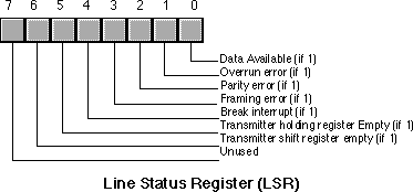
The data available bit is set if there is data available in the Receive
Register. This also generates an interrupt. Reading the data in the Receive
Register clears this bit.
The 8250 Receive Register can only hold one byte at a time. If a byte arrives
and the program does not read it and then a second byte arrives, the 8250
wipes out the first byte with the second. The 8250 SCC sets the overrun
error bit when this occurs. Reading the LSR clears this bit (after reading
the LSR). This error will generate the high priority error interrupt.
The 8250 sets the parity bit if it detects a parity error when receiving
a byte. This error only occurs if you have enabled the parity operation
in the LCR. The 8250 resets this bit after you read the LSR. When this error
occurs, the 8250 will generate the error interrupt.
Bit three is the framing error bit. A framing error occurs if the 8250 receives
a character without a valid stop bit. The 8250 will clear this bit after
you read the LSR. This error will generate the high priority error interrupt.
The 8250 sets the break interrupt bit when it receives the break signal
from the transmitting device. This will also generate an error interrupt.
Reading the LSR clears this bit.
The 8250 sets bit five, the transmitter holding register empty bit, when
it is okay to write another character to the Data Register. Note that the
8250 actually has two registers associated with the transmitter. The transmitter
shift register contains the data actually being shifted out over the serial
line. The transmitter holding register holds a value that the 8250 writes
to the shift register when it finishes shifting out a character. Bit five
indicates that the holding register is empty and the 8250 can accept another
byte. Note that the 8250 might still be shifting out a character in parallel
with this operation. The 8250 can generate an interrupt when the transmitter
holding register is empty. Reading the LSR or writing to the Data Register
clears this bit.
The 8250 sets bit six when both the transmitter holding and transmitter
shift registers are empty. This bit is clear when either register contains
data.
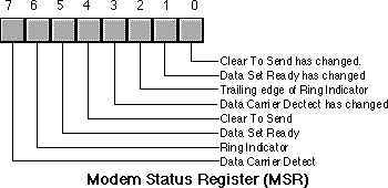
The Clear To Send bit (bit #4) is a handshaking signal. This is normally
connected to the RTS (Request To Send) signal on the remove device. When
that remote device asserts its RTS line, data transmission can take place.
The Data Set Ready bit (bit #5) is one if the remote device is not busy.
This input is generally connected to the Data Terminal Ready (DTR) line
on the remote device.
The 8250 chip sets the Ring Indicator bit (bit #6) when the modem asserts
the ring indicator line. You will rarely use this signal unless you are
writing modem controlling software that automatically answers a telephone
call.
The Data Carrier Detect bit (DCD, bit #7) is another modem specific signal.
This bit contains a one while the modem detects a carrier signal on the
phone line.
Bits zero through three of the MSR are the "delta" bits. These
bits contain a one if their corresponding modem status signal changes. Such
an occurrence will also generate a modem status interrupt. Reading the MSR
will clear these bits.