=============================
= FM TRANSMITTER 3 - 3.5 W =
= Type 1
=
========Version 1.00=========
25-01-94
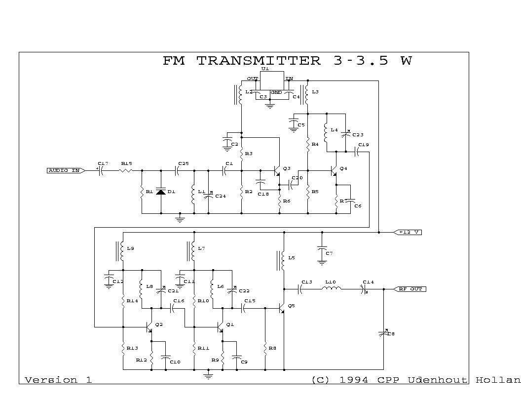
This package contains the schematic for an FM transmitter with 3 to 3.5 W output power, and can be used between 90 and 110 Mhz. Although the stability Although the stability isn't so bad, a PLL can be used on this circuit.
This is a circuit that I've build a few years ago for a friend, who used it in combination with the BLY88 amplifier to obtain 20 W output power (for that schematic, get the LINBLY88.EXE file). From the notes that I made at the original schematic, it worked fine with a SWR of 1 : 1.05 (quite normal at my place with my antenna). He didn't use it for stereo broadcasting, but that shouldn't be a problem.
BTW: I'm sorry about the mess my OrCAD Annotate made of the component numbers.
2) Components/Hints
I don't have a PCB-layout for it, but as I remember I've made it on a normal RF-testing breadboard (with one side copper). Make some connections between the two sides. Build the transmitter in a RF-proof casing, use good connectors and cable, make a shielding between the different stages, and be aware of all the other RF-rules of building.
Q1 and Q5 should be cooled with a heatsink. The case-pin of Q4 should be grounded.
Adjustments:
C24 is for the frequency adjustment. The other trimmers must be adjusted to maximum output power with minimum SWR and input current.
3) Problems?
If you have certain problems, you have to try to solve them yourself first.
But if no solutions can be found you can contact me, so we can try to work it out. This circuit is build by me and it works.
You can also contact me if you have some interesting schematics or material, use E-mail: ericg@stack.urc.tue.nl (at least untill October 1994).
Ofcourse you can use the same adress for other questions or comments on this schematic.
Eric van Gorkom
Component list of the 3 - 3.5 W FM transmitter (Type 1)
Resistors:
(All resistors are 1/4 W carbon or metalfilm types)
R1 :  10k    R6 : 680E     R11: 680E
R2 :  22k    R7 : 150E     R12: 100E
R3 :  22k    R8 : 100E     R13: 3.9k
R4 :  10k    R9 :  68E     R14:  10k
R5 : 3.9k    R10: 6.8k     R15:  10k
Capacitors:
C1 : 4.7 pF ceramic     C11: 100 nF ceramic      C21: 40 pF trimmer
C2 : 100 nF ceramic     C12: 100 nF ceramic      C22: 40 pF trimmer
C3 : 100 nF ceramic     C13:  82 pF ceramic      C23: 40 pF trimmer
C4 : 100 nF ceramic     C14:  60 pF trimmer      C24: 40 pF trimmer
C5 : 100 nF ceramic     C15:  27 pF ceramic      C25:  5 pF ceramic
C6 :  10 nF ceramic     C16:  22 pF ceramic
C7 : 100 nF ceramic     C17:  10 uF/25V
C8 :  60 pF trimmer     C18:  33 pF ceramic
C9 :  10 nF ceramic     C19:  18 pF ceramic
C10:  10 nF ceramic     C20:  12 pF ceramic
Inductors:
L1 : 5 wdg, dia 6 mm, 1 mm CuAg, space 1 mm
L2 : 6-hole ferroxcube wideband HF-choke (5 wdg)
L3 : 6-hole ferroxcube wideband HF-choke (5 wdg)
L4 : 1.5 wdg, dia 6 mm, 1 mm CuAg, space 1 mm
L5 : 6-hole ferroxcube wideband HF-choke (5 wdg)
L6 : 1.5 wdg, dia 6 mm, 1 mm CuAg, space 1 mm
L7 : 6-hole ferroxcube wideband HF-choke (5 wdg)
L8 : 1.5 wdg, dia 6 mm, 1 mm CuAg, space 1 mm
L9 : 6-hole ferroxcube wideband HF-choke (5 wdg)
L10: 8 wdg, dia 5 mm, 1 mm CuAg, space 1 mm
Transistors:
Q1 : 2N3866
Q2 : 2N2219A
Q3 : BF115
Q4 : 2N2219A
Q5 : 2N3553
Others:
D1 : BB405, BB102 or equal (most varicaps with C = 2-20 pF (approx) will do)
U1 : uA78L08, uA7809, uA7810 or equal (MC78LXX, UC78LXX etc)