Originally appeared in Social Defense Mechanisms: Tools for Reclaiming our Personal Space by Limor Fried.
Technical notes for the Fresh Air project.
Introduction: Jamming Techniques
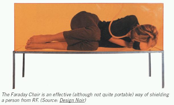
There are multiple ways to incapacitate or jam an RF device. The three most common techniques can be categorized as 'spoofing,' 'denial of service,' and 'shielding' attacks. The first technique basically involves tricking the device into disabling itself or turning itself off. For example, GPS receivers determine their location by listening for satellite-transmitted time codes and performing a triangulation-like calculation. If one could send conflicting time code messages to a GPS receiver, it may compute an incorrect coordinate or malfunction in some other way. One could also construct a device that mimics a cell phone tower. Any cell phone in the area would transmit cell messages to the tower, which the tower would simply 'throw away.' The second technique, 'denial of service' (often referred to as DoS), is more of a 'brute force' method. In this attack the jammer overwhelms the radio band with junk signal, so that any real signals will be drowned out. The third, traditionally known as TEMPEST or EMF shielding, is passive, and basically requires enclosing the area in a faraday cage made of conductive mesh. Any devices inside the cage (which can be as large as a building) will not be able to transmit or receive RF signal outside of it.
All three have advantages and drawbacks. The first technique, 'spoofing,' is much more sophisticated, requiring specialized technology that is customized to each application. It is harder to detect than the other techniques because the jammer is effectively indistiguishable from what it is immitating. The second technique, DoS, is fairly simple, but can be hard to control, (i.e. it is not selective at all, wiping out all devices operating on a certain RF band) and requires a lot of power as it must be many times more powerful than any of the devices being jammed. The third technique, 'shielding,' is the simplest, and is also the only one that complies with FCC regulations. It also requires no power. However, shielding techniques are constrained to a certain location and cannot be used selectively. A faraday shield is always on and tends to affect multiple RF bands.1 Since the Wave Bubble device is meant to be low cost, portable, and adjustable for multiple bands, the most reasonable design would be based on the second technique.
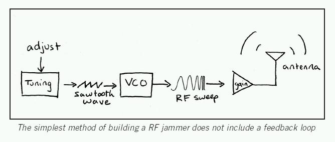
Implementing a DoS attack on RF in hardware is fairly straight forward, the design is essentially the same as that of what is being blocked except much noiser. The main components of a jammer are a voltage controlled oscillator (VCO), a tuning circuit for controlling the VCO so as to transmit into the desired RF band, a 'noise' source which may be built into the tuning circuit, an RF amplification circuit (otherwise known as a 'gain stage'), and an appropriate antenna. All of these components are now mass-manufactured as solid-state devices, are low cost (totalling under $50), and can be packaged into a portable device.
VCO Selection
At the heart of the RF jammer is a VCO, the device that generates the RF signal which will interfere with the cellphone, GPS receiver, etc. There are three selection criteria for selecting a VCO for this application. Most importantly it should cover the most popular bands that a user may want to defend him or herself from. These are the mobile phone AMPS (800 MHz), PCS (800 MHz, 1800 MHz, and 1900 MHz), and GSM (900 MHz, 1800 MHz and 1900 MHz) networks, GPS (1227 MHz and 1575 MHz), WiFi (2.4 GHz) and the most popular RFID spectrums which include 14 MHz, 400 MHz, 800 MHz, and 2.45 GHz. Secondly, it should be readily available at low cost and in small quantities. Third, it should be in small enough a package to allow portabilization. Lastly, it is preferable for the device to have reasonable power requirements. That is, it should run at low control voltages and with low power consumption.
Low frequency VCOs (under 1 MHz) are somewhat simple to build using opamps, and are often implemented as RC relaxation circuits. High frequency VCOs (above 10 MHz) are more complicated in their design, and are often based on Clapp or Colpitts oscillators. Since we are concerned with RF in the range of 800 MHz up to 2.5 GHz, a wide-band, high-frequency VCO is desired. Inquiries into various VCO technologies have resulted in a three viable options: building a VCO from 'scratch,' purchasing a 'encased' VCO from an RF parts supplier, or using a VCO with built-in phase-locked loop (PLL, basically a feedback-driven tuning circuit) such as those available from Analog Devices.
Building a VCO from scratch is not particularly difficult, as there are only a dozen parts required, but involves a great deal of consideration over component selection to acheive proper functionality. The benefits of constructing the VCO include extremely low cost (on the order of a dollar or two), versatility (the VCO can be designed with a custom range) and availability (since it uses only a few transistors, and readily available passive components). Unfortunatly, the actual construction is very difficult to debug without proper equipment or expertise.
Prefabricated VCOs (the second option) are essentially the same topologicaly as hand-made ones, except that the fabrication and testing work is done by a company. These VCOs are often just small circuit boards with Clapp/Colpitts oscillators built onto them, then hermetically sealed into a metal case. The main benefit of going with this option is a guarantee of functionality, although at the loss of RF band-selection and at an increased price. The third option is a fairly new technology - only recently have IC manufacturers begun combining VCOs into their PLL chips. The benefits of such a device include having a high quality tuning circuit built in, which saves costs and eases some parts of the fabrication process. However, it also means that there must be a microcontroller included into the design to control the embedded digital PLL (the other two options use a simple voltage tuning circuit). Also, such chips tend to have much narrower bandwidths, roughly 100 MHz.
At the time of development, Analog Device was the only company with combined VCO/PLL synthesizer chips, produced under the ADF4360 series name. While these chips are fairly inexpensive and low power, they also have low output power and low bandwidth. To cover the desired RF spectrum, three chips would be necessary. The ADF4360-7 (350-1800 MHz) covers the GPS bands and lower cell bands, the ADF4360-3 (1600-1950 MHz) covers the upper cell bands, and the ADF4360-1 (2040-2450 MHz) covers the WiFi and BlueTooth bands. Many of the chips were not yet in wide-spread production and were difficult to obtain during the design and specification phase of this project. Therefore, they were not fully explored as a viable option.
I then decided to explore constructing and designing my own VCOs, so that I could customize the RF band output. A wideband 1-2 GHz design based on a Colpitts/varactor VCO was built and tested. While the design seemed sound, I could not get the VCO to oscillate past 1.5 GHz, much lower than expected or desired. Lacking suitable equipment and expertise to fully debug the circuit, I opted to pass on working further on this topic, noting that if I were designing RF jammers for sum 1.5 GHz signals, hand-built VCOs are a viable option.
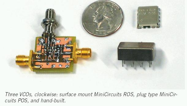
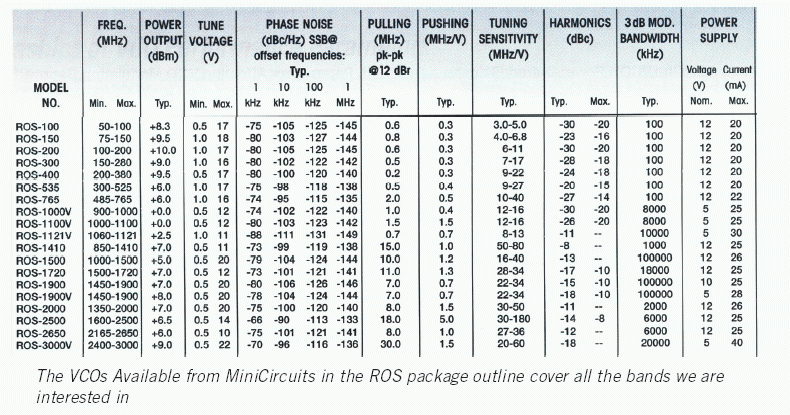
Finally, I decided to go with prefabricated VCOs. Although they are more expensive than the rest of the options, they are guaranteed to work and are not prohibitively expensive. There are easily a dozen companies producing fabricated VCOs, but the two companies whose products I found to be the most available were Micronetics and MiniCircuits. Micronetics makes high quality parts, and an early version of the Wave Bubble uses one of their VCOs. However, I found MiniCircuits to provide an much wider range of VCOs at lower prices. I chose the ROS line of VCOs, as that line seemed to cover a good wide range of RF bands covered with reasonable power requirements, in a small but managable package. In particular, I intended to use the ROS-2500, with a frequency range of 1.5 GHz to 2.5 GHz, and the ROS-1410, with a frequency range of 800 MHz to 1.4 GHz. Combined, these two VCOs cover all but the low RFID frequency ranges. The RF power output of this range of VCOs is on the order of +7 dBm. The power requirements are modest, around 25 mA at 12V. The output frequency is programmed via an analog input voltage, ranging from 0 to as high as 25V.
Tuning Circuitry
The tuning section of the RF jammer sweeps the VCO through the desired range of frequencies. There are two commonly used types of tuners: open-loop and feedback. The first kind of tuner is very simple, and requires only a few op-amps and passive components. Basically, it is just a triangle or sawtooth-wave generator, offset the proper amount so as to sweep the VCO from the minimum desired frequency to a maximum.2 Often, because VCOs drift with power supply, and because lots can have tuning variations, a frequency-counter or spectrum analyzer is necessary to get the correct bandwidth. The second type of tuner uses a PLL to constantly adjust the VCO to keep it at the right frequency. For such high frequencies, a programmable PLL must be used, whereby the PLL divides down the RF frequency by a 32-bit number n and then compares it to a 'quality' (i.e. high precision) reference frequency from a crystal running at, say, 10 MHz. If the VCO's output frequency is too high, the output pin of the PLL drops low, and vice versa. To program in n, a microcontroller must be used. Since most RF projects have the VCO tuned to a single frequency, the divider, n, is often programmed once and connected more or less directly to the VCO in a feedback loop. Since this is not the situation for us - we would like to sweep the frequencies - the VCO/PLL stage requires a more complicated setup involving a microcontroller and possibly digital potentiometers. For this revision, only a simple tuner was implemented, with the intention that future revisions will include self-tuning/PLL circuits.
Gain Stage and Antenna Selection
In order for Wave Bubble to protect its user's personal space, it must effectively disable RF communication in a fairly large area. The target radius of the Bubble's jamming area is on the order of 2m, which corollates to the size of the average American's personal space 'bubble.' Once the VCO has been chosen, the output power of the jammer (which is proportional to the effective area) can be increased by adding amplification stages before the antenna. Each gain stage increases the output power (up to a certain maximum defined by the maximum capable by the gain stage) at the cost of battery life.
For the gain stage, I chose the AG-603 InGaP gain block, an easily available, general purpose RF buffer amplifier. In general, the AG-603 has an ft at 6 GHz, and provides about 17 dB gain or more up to 2 GHz, which suits us well. The IC is linearly biased from a 6V rail through a resistor, and draws 75 mA, consuming a little less than half a Watt. The maximum output power of this particular device is a little more than +20 dBm which means that, given our VCO output power of +7 dBm, using one gain stage is fine, but that it is not possible to cascade two or more. If more output power is desired, a second, higher-power amplification device will be required. Early prototypes using a single gain stage proved to be successful in disabling cell phones at 2m distance, and so a higher powered gain stage was not investigated.
A proper antenna is necessary to propagate the jamming signal. In order to have optimal power transfer, the antenna system must be matched to the transmition system. Matching the antenna is usually just a matter of picking an antenna with little return loss, usually described as the VSWR. A well-tuned antenna, one that has a VSWR of 3 or less at the transmitted frequencies, is highly desirable. For the first few revisions of the Wave Bubble, all of which operated in the PCS or GSM bands, a GSM patch antenna was used. Such antennas are soldered directly to the PCB and are quite small. Unfortunatly, patch antennas come in various sizes and mounting patterns and are not, in general, interchangable. Since the Wave Bubble is intended to be tunable to any frequency, the patch antenna was later replaced with an RP-SMA PCB edge-launch connector so that a variety of antennas may be attached depending on what frequency band the device is tuned for.
Power Supply
For Wave Bubble to be an effective portable RF jammer for daily use, it must have enough power to jam RF in the vicinity of the user, and go without recharging for at least a day or two. All RF jammers require a lot of power as, by definition, they must substantially overpower all nearby devices to disable them. Therefore, the most important specification of the Wave Bubble power supply was that it would provide the almost 2W of power required, for at least 2 hours of use (enough to last through an entire movie, or meal at restaurant) at a fairly low cost and in a reasonable amount of space.
Unfortunatly, the Wave Bubble requires three different voltages to run, two of which draw a fair amount of current. These requirements make the power supply design particularly complex. Depending on what model is used, the VCO may require up to 40 mA at 12V. (The two particular VCOs chosen for this design both ran at 12V at 25 mA each.) Each RF gain stage requires 6V at 75 mA, with at least one stage required per VCO. The VCO tuning circuit runs mostly at 6V, at a few mA, but also requires up to 30V to tune the VCO over its entire range.
Since the device is intended to be used on a daily basis it must run either on a rechargable battery pack or disposable batteries, both of which usually average 3-5 VDC at a few Ah. Therefore, DC-DC step-up converters must be used to provide the high voltages necessary to run the device. The two options for such converters are inductor-based boost regulators and switched-capacitor voltage doublers. Switched-capacitor converters are fairly simple and reasonably effecient, but are not regulated (that is, if you want 5V from 3V you have to double to 6 and then use an LDO regulator to get 5V). Boost converters are always regulated, but cost a little more, and are more complex to get working, requiring careful specification of the external components to acheive high efficiency.
The first design of the Wave Bubble power supply utilized a dual boost regulator, the LT1944 from Linear, to generate +-12V and 6V. Although this solution was functional, it operated at the edge of the converter s capabilites. Another issue that cropped up was that, depending on the PCB layout, RF noise would couple into the inductors, saturating the cores and causing the boost regulator to fail intermittantly. A second power supply was designed, using only switched-capacitor DC-DC converters. Such converters would be immune to failure inductor saturation. A three-voltage (+6, +12 and +24V) switched-capacitor power supply was designed for Wave Bubble.
Unfortunatly, there are many drawbacks to using switched-capacitor converters. First, they are often configurable only as voltage doublers or inverters which means that three cascaded converters are necessary. Secondly, they are often not regulated and have fairly high output impedance, which means that a separate voltage regulator is needed for each voltage output stage. What this amounts to is that the cost of the power supply is quite high and many components are necessary. However, unless a proper shielding system is built, this type of supply is the only one that can provide guaranteed performance.
To power Wave Bubble, a fairly powerful battery source is needed. Two viable sources are 2-4 standard AA alkaline batteries, or a medium-sized (3.7V at 1 Ah) lithium ion battery. Either will suffice to run Wave Bubble for multiple hours.
Conclusion
The Wave Bubble was designed and built during the spring term of 2004. Multiple revisions were tested against different cell phones with reasonable success. Older (2nd generation) cell-phones were easier to jam, likely because their output power is lower, and their receiving front-end less sensitive than those of current phones. Depending on the cell phone model, the effective zone of the bubble ranges from 1 to 2m. While the design is successful, there is a lot of work that needs to be put into Wave Bubble before it can be considered completed.
Improvements
There are many possible improvements that can make Wave Bubble more effective and reliable. The most important is the design and implementation of a simple power supply, a task that is not difficult as much as tedious. It seems likely that a fully switched-capacitor power supply would be best, to minimize failure due to a poorly shielded board. Unfortunatly, there are multiple versions of switched-capacitor chip, each with different loads and capacities. It seems that, considering the large number needed to run Wave Bubble, it might be best to implement all of the DC-DC converters using a 3-channel PWM chip. Particularly if it is possible to hand-build a chargepump converter that can supply more than 200 mA, a bottle-neck in the current revision.
There is also an obvious need for a feedback tuning circuit; few people have RF frequency analyzers for tuning the jammer by hand. A good candidate for a PLL is the LMX23xx seriers of high frequency, programmable PLLs. This chip would have to be programmed every time the device is turned on, likely by a microcontroller. Instead of a passive feedback loop, the microcontroller could use programmable resistors to set the bandwidth and offset. Such a setup would make it easy to change the configuration of the jammer on the fly, i.e. have a switch for selecting which band the user would like to disable.
Appendix A