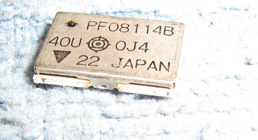
Overview of the Renesas/Hitachi PF08114B MOSFET RF power amplifier module.
They are available on eBay for around $4 each.
It's in a 10-pin surface-mount package.
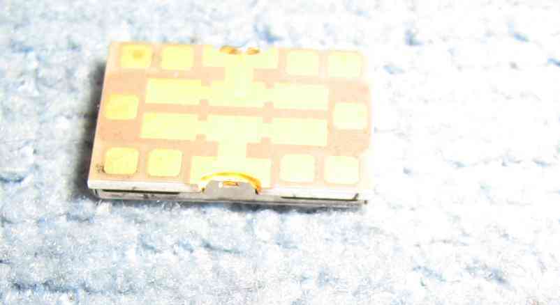
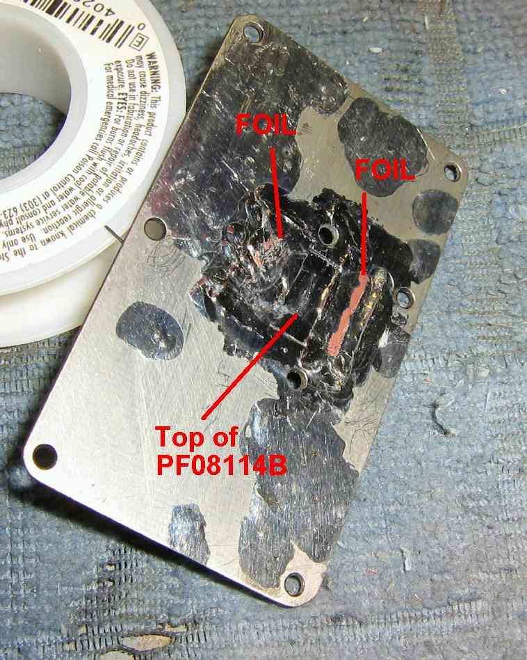
Bottom view of the Renesas/Hitachi PF08114B MOSFET RF power amplifier module.
Making a proper PC board for this device would require alot of work, but we can improvise something cheaper by mounting the device upside down.
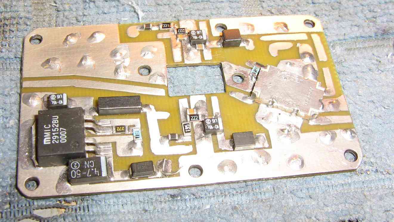
Making the PC board for the amplifier.
Proper microwave construction techniques will be required. Use quality doubled-sided FR4 material with lots of vias connecting the ground planes.
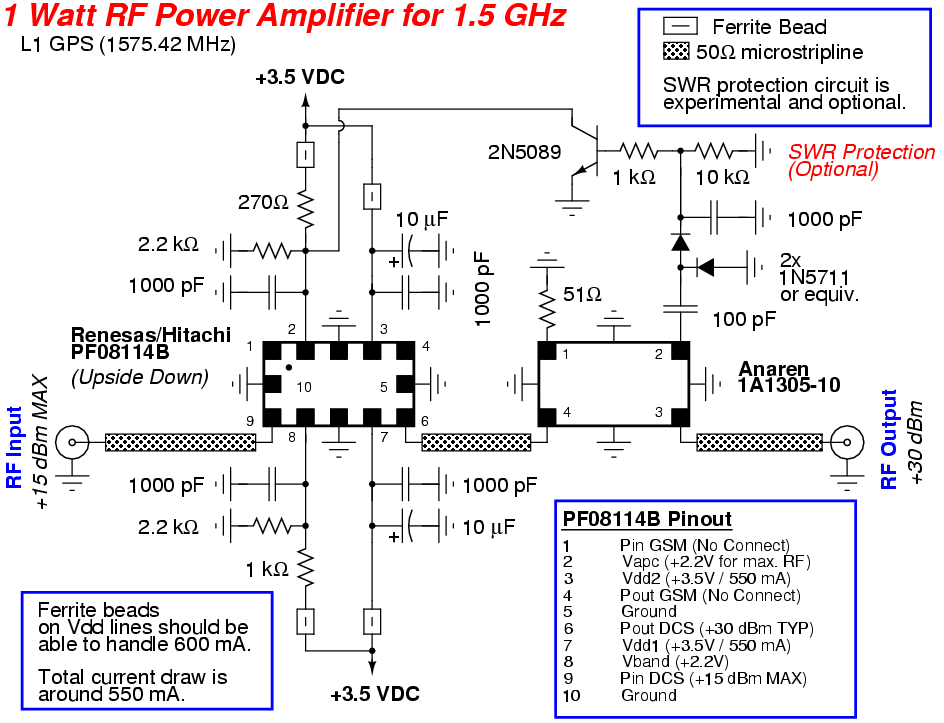
The voltage regulator is a Micrel MIC29152BU configured for a +3.5 VDC output. The R1 resistor is 2700 ohms (1%) and the R2 resistor is 1500 ohms (1%). Refer to the MIC29152BU's datasheet for more information on tweaking the output voltage value.
Be sure the ferrite beads on the PF08114B's Vdd power lines are capable of handling 600+ mA without saturating or dropping too much voltage.
An experimental SWR protection circuit was added to this design, but it doesn't work quite like I wanted.
An Anaren 1A1305-20 20 dB directional coupler detects the reflected power and pulls the PF08114B's Vapc line down in a high SWR condition. The 20 dB coupler doesn't quite have enough coupling power for this low-power amplifier. A 6 dB (1A1305-6) or 10 dB (1A1305-10) coupler should be used instead.
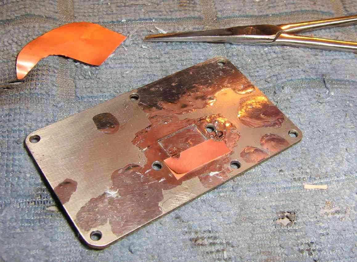
Mounting the Renesas/Hitachi PF08114B MOSFET RF power amplifier module.
It's placed upside down into the cutout made in the PC board.
Solder-tin the PF08114B's (top) case and add little strips of thin copper foil to connect the PF08114B's case to the ground plane of the amplifier circuit board. The thin copper foil can be found at most hobby stores.
Doing this helps to properly ground the PF08114B and also acts as a makeshift heatsink.
Finished overview of the PF08114B installed in the amplifier circuit board.
Be sure the bottom of the board is very smooth. Use the side of the soldering iron to "smooth" out the solder.
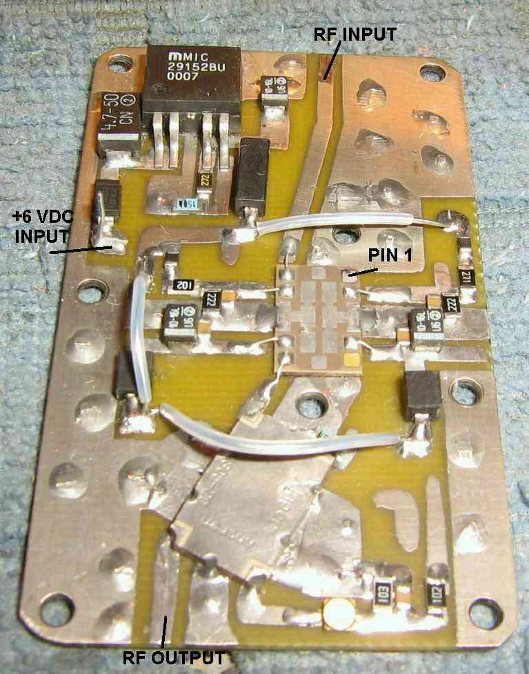
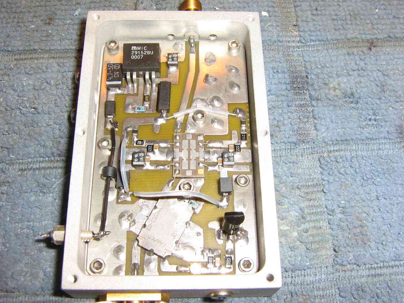
Completed amplifier circuit board overview.
The RF input (1575.42 MHz / +10 dBm typical, +15 dBm maximum) is via that top trace.
The RF output (approximately +30 dBm) is via the bottom trace.
Small #30 gauge wire jumpers connect the PC board traces to the proper PF08114B pads. Be sure to note "pin 1" when the PF08114B is upside down!
The SWR protection components where not installed yet, as this circuit was still experimental.
The detection diodes may need a little bit of forward bias, depending on which ones you use. This can be done with a simple two resistor voltage divider at around 0.2 volts.
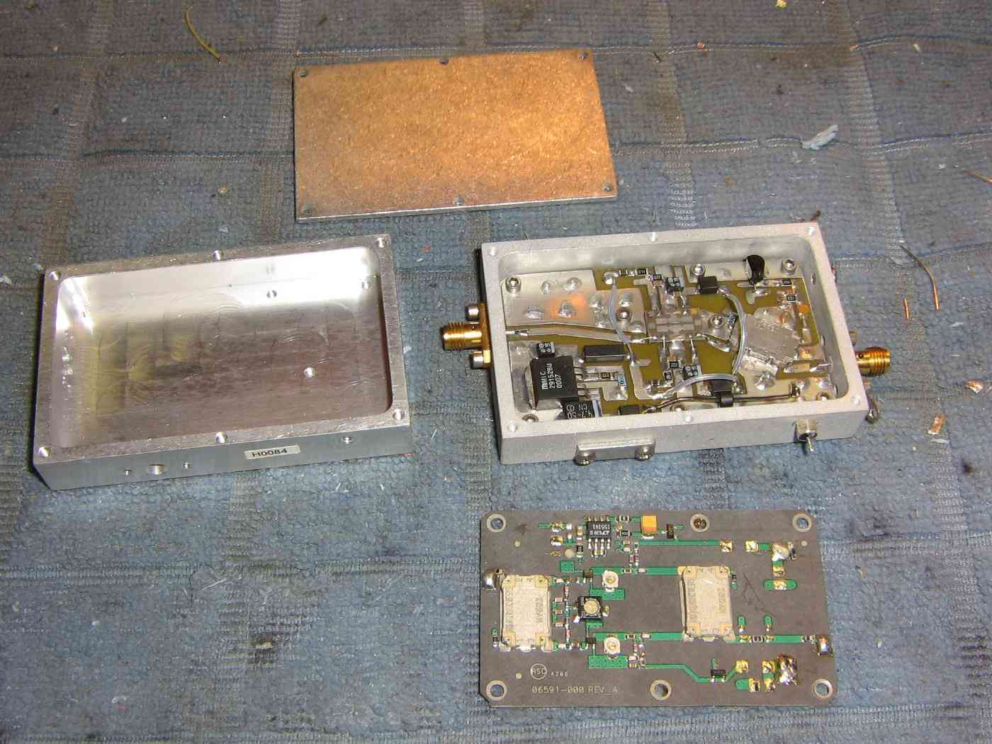
Mounting the 1 watt RF amplifier circuit board into the case from an old cellular phone (800 MHz) receive pre-amplifier.
SMA connector are used on the RF input/output.
You can power the RF amplifier from any +6 to +12 VDC power source capable of around 600 mA continuous.
Completed overview.
Be sure the case which you mount the circuit board to is capable of acting as a heatsink.
Two extra #2-56 screws were added off to the sides of the PF08114B. These are to help ensure the PF08114B is properly heatsinked and grounded to the aluminum case.
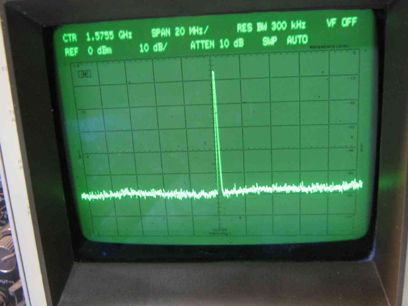
Testing the RF amplifier at 1575.42 MHz with a 0 dBm (1 mW) RF input.
The reference line is 0 dBm at there is 30 dB of attenuation on the spectrum analyzer's input.
No oscillations or spurs were detected.
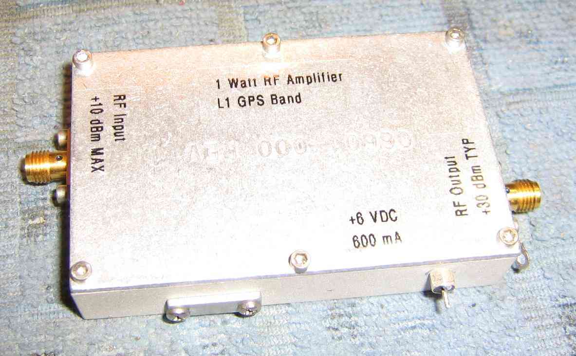
Completed case overview.