The second part of the GBPPR Non-Linear Junction Detector project will be constructing the first local oscillator/mixer and the transmitter circuits. While these would have been difficult circuits to construct just a few years ago, the availability of pre-built synthesizer modules significantly increases the ease of construction. A Mini-Circuits DSN-2300A-1119 1690 to 2310 MHz frequency synthesizer will be used for the first local oscillator and a Z-Communications PSN0930A 900 to 960 MHz frequency synthesizer will be used for the transmitter's main oscillator.
Those synthesizers are programmed using the standard three-wire serial interface (Data, Clock, Load Enable). The DSN-2300A-1119 is based around the Analog Devices ADF4106 PLL, while the PSN0930A is based around the National LMX2316 PLL. Both of those PLL chips are programmed in a quite similar fashion (by loading an initialization/function register, a "R" divider register, and a "N" divider register), but the specific bit values will be different. The Z-Comm PSN0930A is designed for 100 kHz tuning steps and the Mini-Circuits DSN-2300A-1119 is designed for 250 kHz. Those are both fixed step values and you'll need to take this into account when programming the synthesizer's final frequency.
The PLLs will be programmed using a BASIC Stamp 2 controller. I'm still working on the actual "software" of the NLJD, but some example code will be given for those wishing to experiment.
The first local oscillator will switch between 2240 and 2270 MHz to receive the 2nd or 3rd harmonic. This signal will directly feed the LO port on a Mini-Circuits SRA-3500 mixer. The 436 MHz IF output from the SRA-3500 mixer will be amplified around 18 dB by a WJ Communications/TriQuint AH31 high-dynamic range IF amplifier and bandpass filtered by a Toko 492S-1055A filter.
The two hopping local oscillator signals will generate a 436 MHz IF output with a RF input frequency of either 1804 MHz, the second harmonic of the 902 MHz illumination carrier (2240 - 1804 MHz) or 2706 MHz, the third harmonic of the 902 MHz illumination carrier (2706 - 2270 MHz).
Both of the frequency synthesizers will be sharing the same 10 MHz TCXO time base. One quirk with the Mini-Circuits DSN-2300A-1119 is its requirement for a reference signal with a "slew rate > 50 V/µS" when operating below 20 MHz. That's just a fancy way of saying the reference signal may need to be a square wave. Everything did appear to test fine with the stock 1 volt peak-to-peak output signal from the EG&G TCXO circuit described earlier.
There were two problems encountered during the construction and testing of the first local oscillator & mixer and transmitter circuits. First, the SRA-3500 I used showed significantly higher conversion loss than it should. The SRA-3500 was salvaged from some other radio gear, so it may have been damaged to begin with. The first mixer's performance is critical in this application and it should have low conversion loss and high isolation on all ports. High conversion loss essentially makes the receiver "deaf" from the get-go.
The second problem was I blew up the Pacific Monolithics PM2111 RF power amplifier while testing the circuit! It does work fine, as long as you follow the PM2111's datasheet closely. I was running the PM2111 from a separate power supply without any current limiting or voltage spike protection and must of just caught it at the wrong moment. The PM2111 "popped" when I flipped on the power and was destroyed. Oh well...
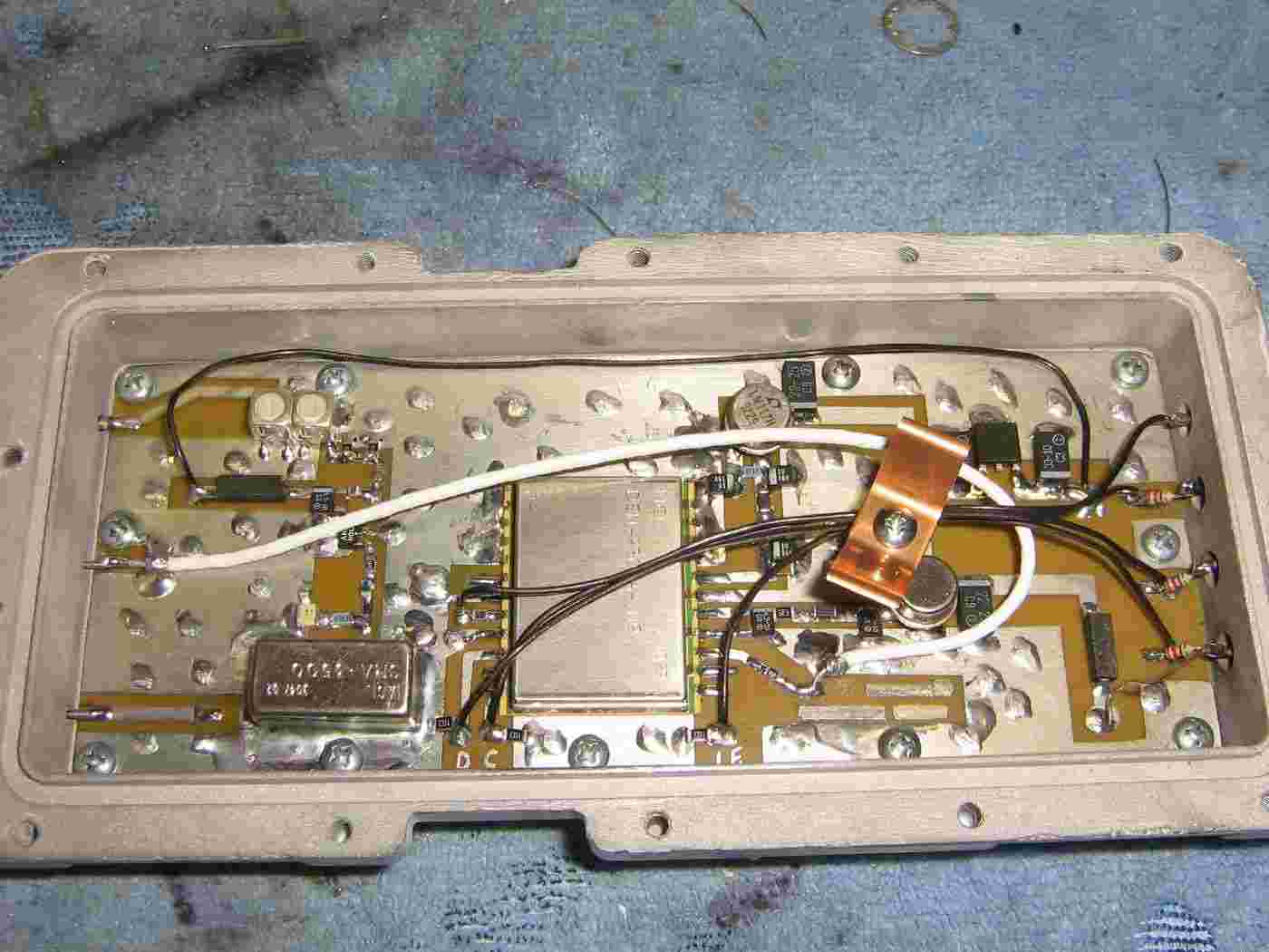
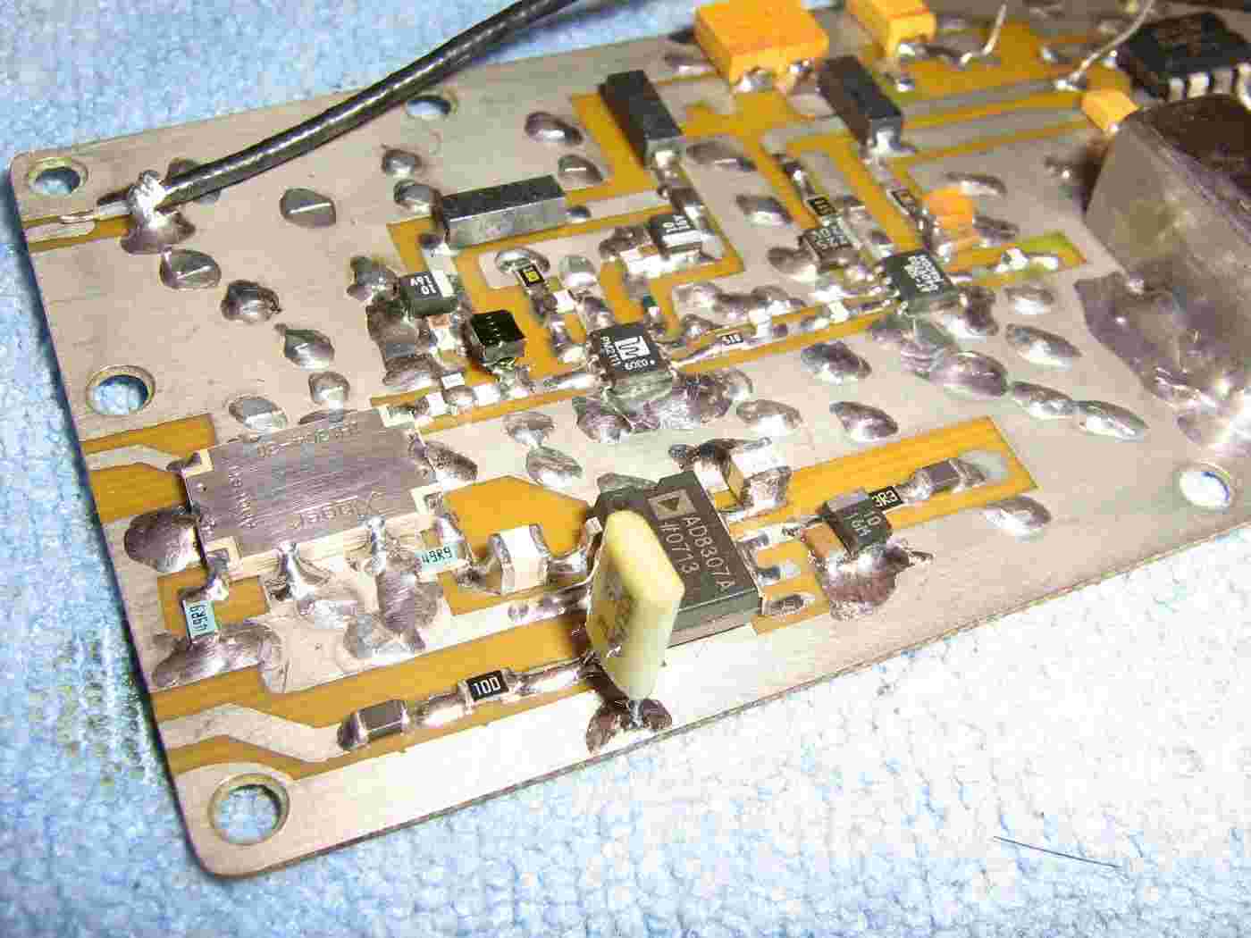
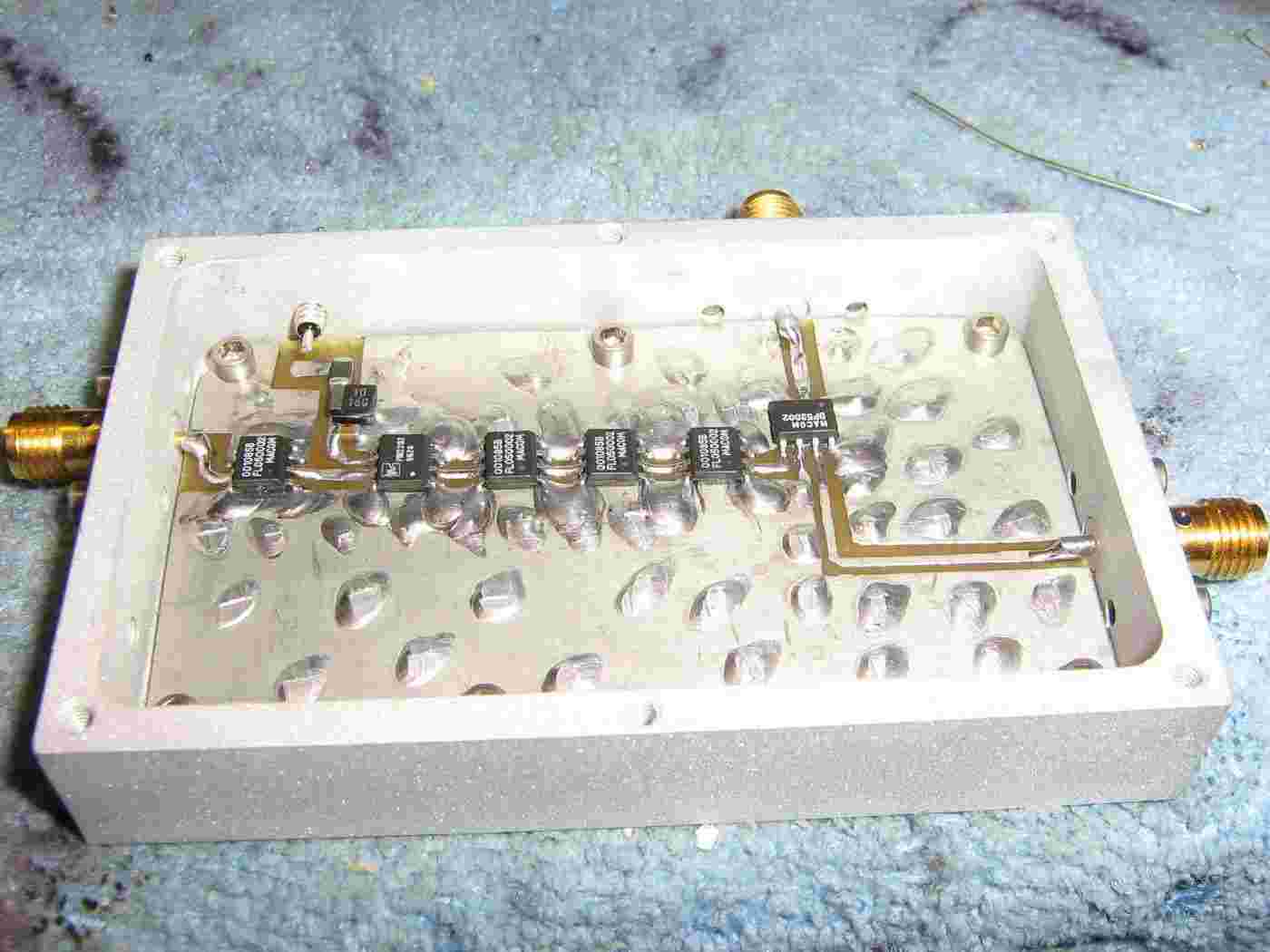
Overview of the first local oscillator and mixer.
What would have been a complicated circuit is now simplified by using a pre-built Mini-Circuits DSN-2300A-1119 synthesizer module.
The Mini-Circuits DSN-2300A-1119 does require a clean source of +5 VDC and +12.5 VDC. These are provided by the LM140 and LM117 voltage regulators on the right side.
The Mini-Circuits SRA-3500 mixer is on the lower-left with the WJ/TriQuint AH31 IF amplifier and Toko bandpass filter just above it.
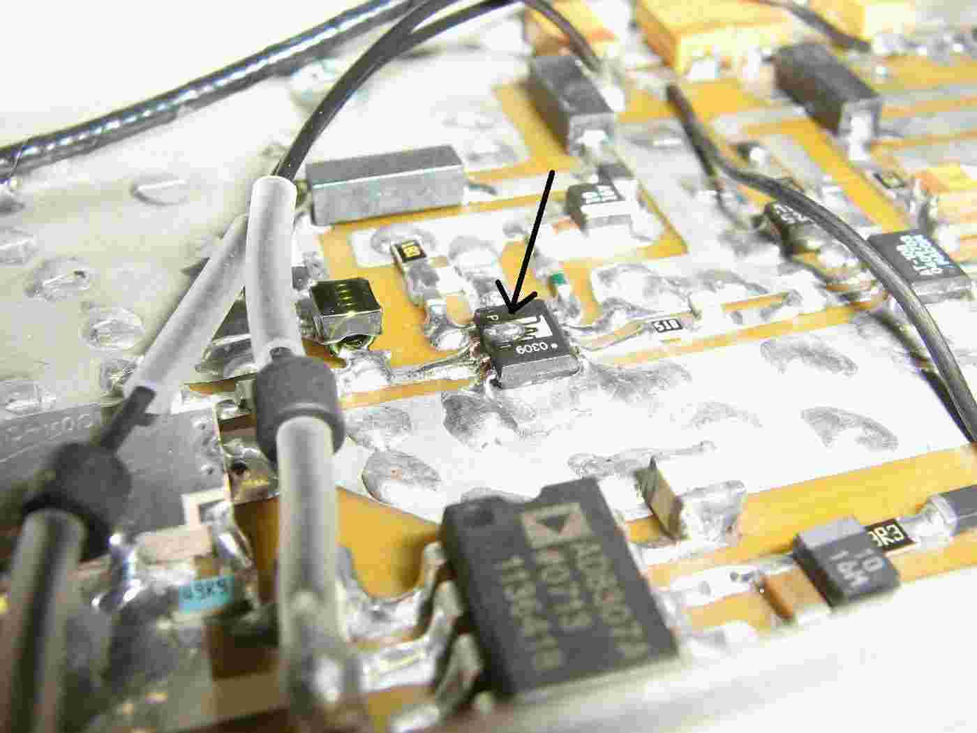
Alternate view.
The 78M05 voltage regulator (lower-left) is only for the WJ/TriQuint AH31 IF amplifier. The AH31 has a fairly high current draw (150 mA) and the series ferrite bead and inductor should be chosen after taking this into account.
The Data, Clock, Load Enable, and Lock Detect signals are routed via the 1,000 pF feed-through capacitors on the left. Four holes where drilled and tapped (#12-32) for the feed-through capacitors.
The Mini-Circuits DSN-2300A-1119 requires "3 volt" level logic signals, so simple resistor voltage dividers are used to convert the 5 volt output logic signals from the BASIC Stamp down to 3 volts.
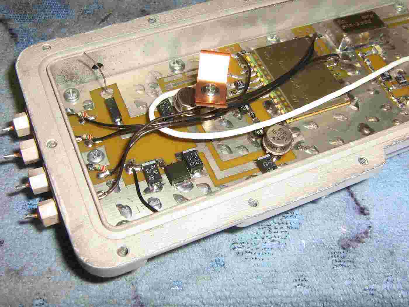
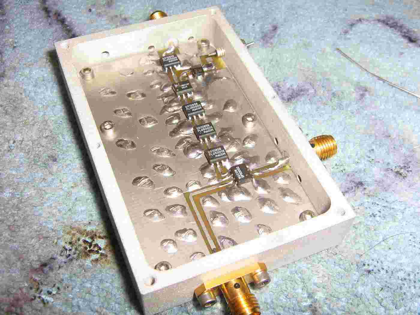
Overview of the Mini-Circuits SRA-3500 mixer and WJ/TriQuint AH31 IF amplifier section.
A simple one-pole diplexer centered at 436 MHz is on the IF output of the mixer.
The WJ/TriQuint AH31 operates at around 150 mA and has it's own voltage regulator. A 3 dB attenuator is on the output of the AH31 to help the IF amplifier and mixer to "see" 50 ohms. Final gain from the IF amplifier circuit was around 14 dB.
The Toko 492S-1055A filter (type 5CHW pinout) was purchased from Digi-Key (Part No. TK5442CT-ND), but it doesn't appear to be available anymore. Any similar bandpass filter (430-450 MHz range) should work. Since the 436 IF frequency we are using is in the middle of the 70 cm amateur radio band, you may be able to salvage similar filters from older radio gear.
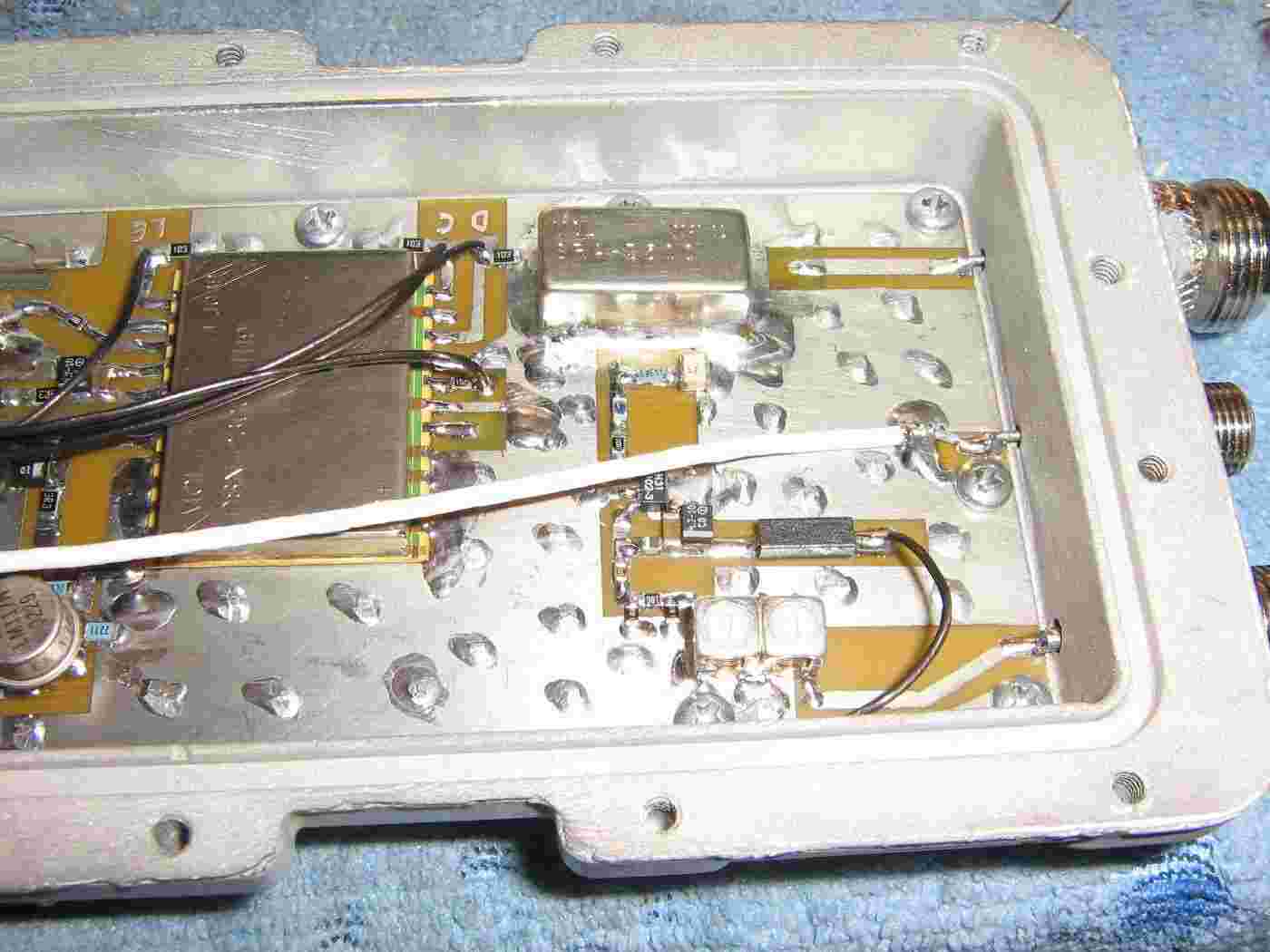
The N connector on the upper-right is the RF input to the mixer. The middle F connector is the 10 MHz reference input for the Mini-Circuits DSN-2300A-1119. The TNC connector on the lower-right is the 436 MHz IF output.
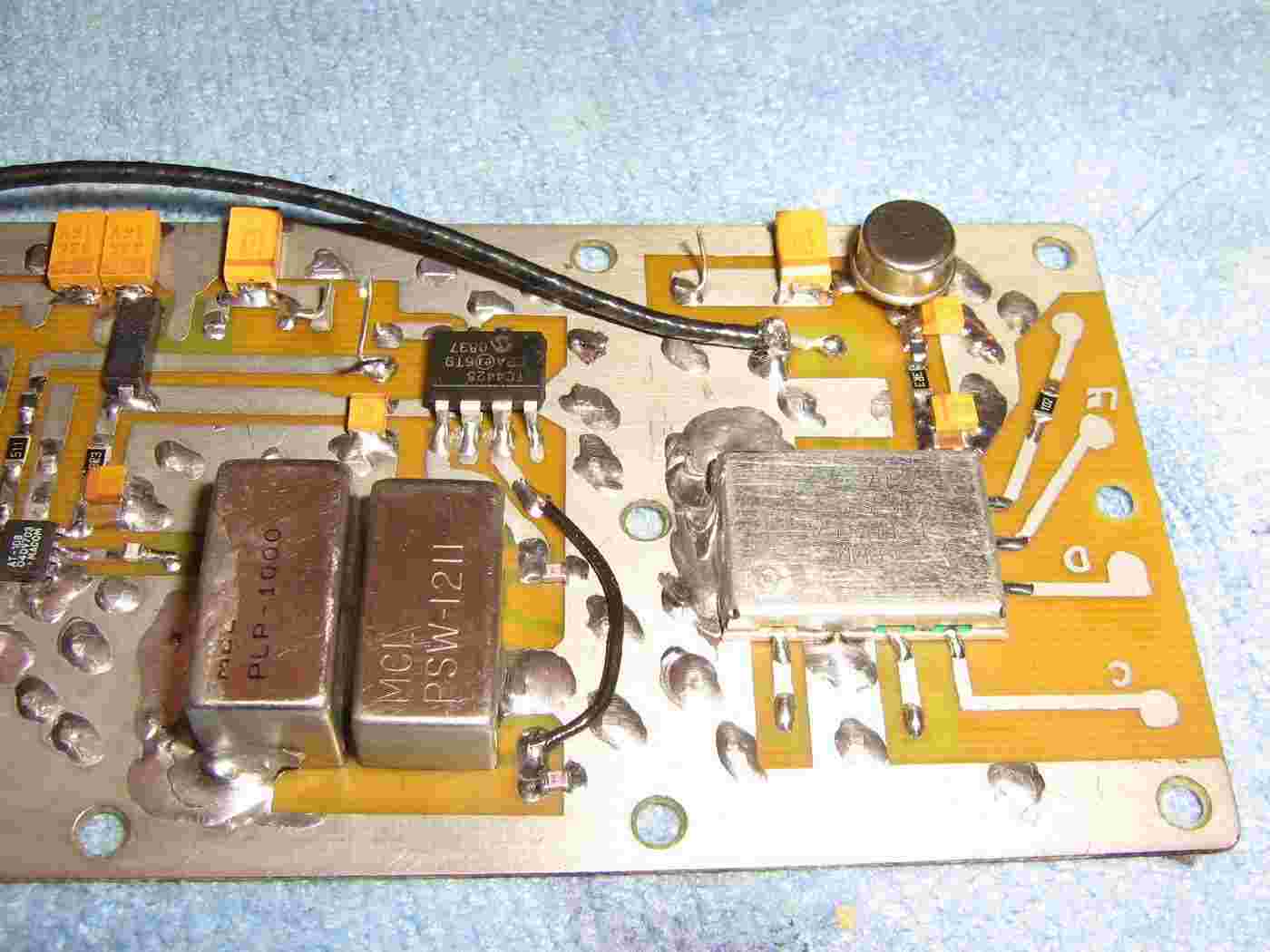
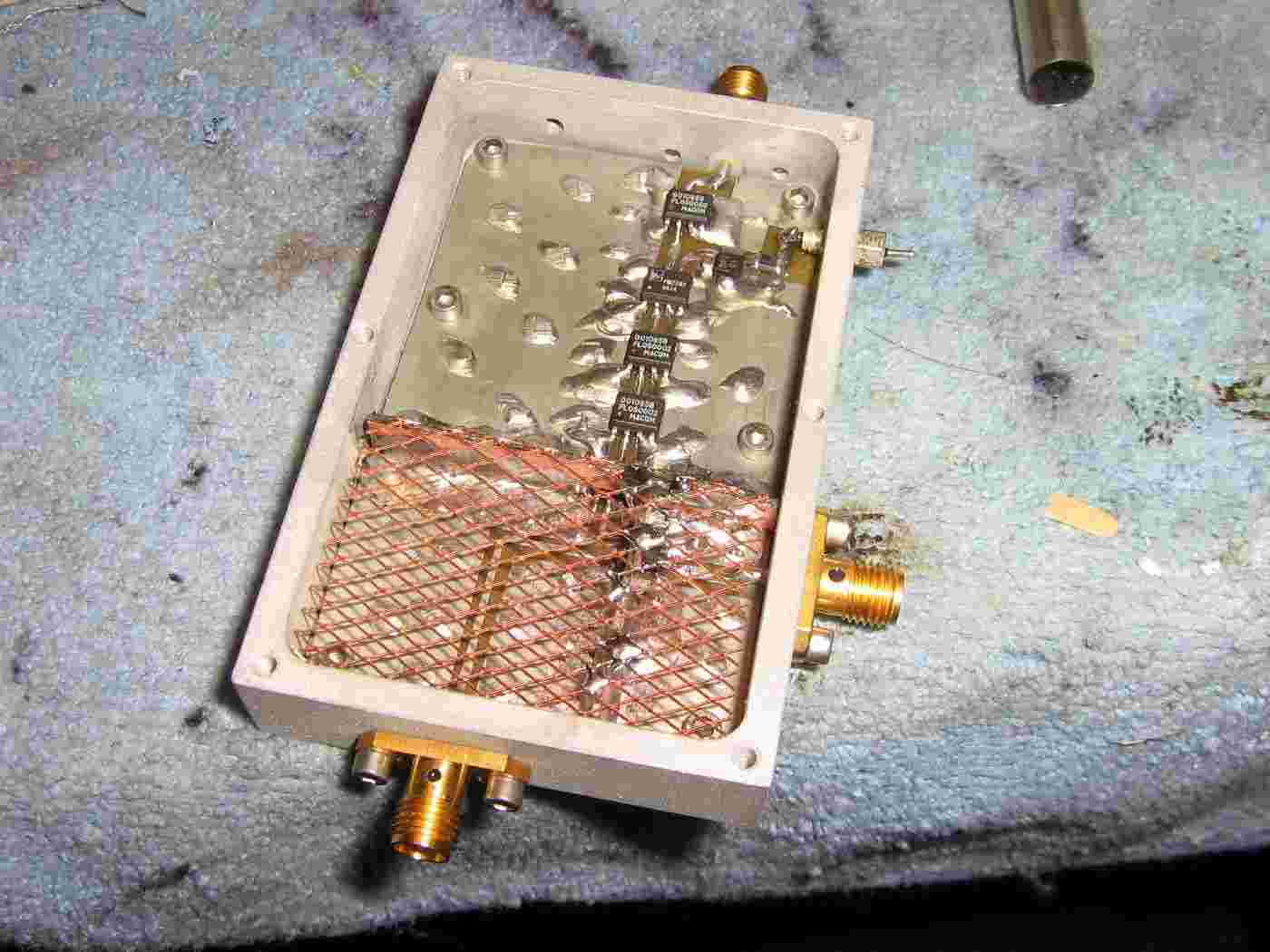
Overview of the transmitter circuit.
The Z-Communications PSN0930A frequency synthesizer module is on the right and is powered from its own LM140 voltage regulator. The 10 MHz reference signal is coming in via the coaxial cable along the top.
On the lower-left, is a Mini-Circuits PSW-1211 PIN diode RF switch and a Mini-Circuits PLP-1000 low-pass filter.
The Mini-Circuits PSW-1211 can be used to "modulate" the main illumination carrier by pulsing it on and off. This is optional, but having an audio tone on the received signal is helpful for detection using only your ears. It's also possible to use the timing of the pulses to locate the distance to the surveillance device your trying to find, but that'll be for another day.
The Mini-Circuits PLP-1000 low-pass filter provides the first round of low-pass filtering to remove any harmonics of the main illumination carrier RF signal.
A Microchip TC4428 dual high-speed power MOSFET driver is used to control the Mini-Circuits PSW-1211 PIN diode RF switch. A panel-mounted SPDT (center-off) switch will select between a CW or 1,000 Hz modulated RF carrier. The center-off position will disable the RF output.
Output of the transmitter circuit.
A M/A-Com AT-108 voltage-variable attenuator is the 8-pin SMT IC on the middle-right. This provides an approximate 0 to 40 dB attenuation range of the transmit RF carrier. This control is done via a panel-mounted potentiometer.
The center 8-pin SMT IC is a Pacific Monolithlics PM2111 800-1700 MHz RF power amplifier - before I blew it up. The PM2111 amplifies the 900 MHz RF carrier around 30 dB for a maximum final RF output power of around 1 watt (+30 dBm). The Pacific Monolithlics PM2111 is linear biased, which is required to reduce the creation of harmonics and to allow low-power signals to drive the PM2111.
Combined with the M/A-Com AT-108, the final RF output power is variable from around -10 to +30 dBm (0.1 mW to 1W).
The RF output from the Pacific Monolithlics PM2111 is taken through an Anaren 1H1304-30 800-1000 MHz 30 dB directional coupler. The output from the directional coupler is sent to an Analog Devices AD8307 logarithmic RF detector for a TX power LED display.
And then it died... Everything did work before this, though. (Video)
Study the datasheet for the Pacific Monolithlics PM2111 very carefully. Be sure the SMT inductors you use have a self-resonant frequency above 900 MHz, and also make sure the 18 nH inductor can handle the high current (620 mA) the PM2111 requires. The capacitors for the PM2111's RF input/output matching section should also be of high-quality.
The PM2111 has a solder tab on the bottom of its IC package. "Pool" a little puddle of solder under the PM2111 using a heat gun, the quickly "drop" the PM2111 into position.
Proper microwave construction techniques must be followed when constructing the transmitter circuit to prevent the PM2111 from oscillating.
There were some small reference spurs +/- 100 kHz of the main RF carrier, but these are at an acceptable level.
Overview of the modified transmitter circuit.
PM2111 with a coax jumper from the output of the AT-108 to the input of the directional coupler.
Below is a chart of the actual RF output power (as low as I could measure) of this circuit with the bypassed PM2111. The PM2111 would have added another 30 dB or so to the final RF output power.
AT-108 Control Voltage    RF Output Power
5.0                       -1.2 dBm
4.0                       -2.5 dBm
3.0                       -12.2 dBm
2.5                       -15.8 dBm
2.0                       -20.0 dBm
The AD8307 provides a 0.5 - 1.6 VDC output indicting the final RF output power. The AD8307 isn't really designed to work at 900 MHz, but it does work. Refer to Figure 45 in the AD8307's datasheet for a graph of output voltage vs. input RF power at 900 MHz. My "blown up" amplifier only reached a peak output voltage of around 0.8 VDC. Remember to make into account the 30 dB loss from the directional coupler.
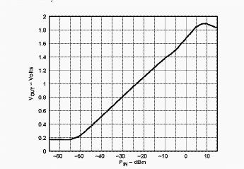
Figure 45: Output vs. Input Level for a 900 MHz Input Signal
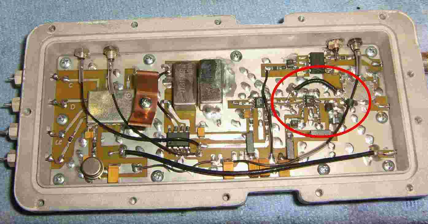
Experimental diplexer and low-noise receive amplifier circuit.
The key to a decent working non-linear junction detector is isolation of the transmitter and receiver. The receiver shouldn't hear the transmitter. Period.
This, of course, turns out to be a big problem in the real-world. There are commercial diplexers ("cans") available which are tuned to allow the transmitter and receiver to share a single antenna, but tend to be expensive, difficult to locate, and even more difficult to homebrew.
Thankfully, the frequency range(s) of this non-linear junction detector fall within the frequency range(s) used by most cellular phones. M/A-Com makes the DP52-0002 diplexer, which is a 8-pin SMT dual-band diplexer that provides a low-pass/high-pass function for 900/1800 MHz cellular phones. This little chip alllows a single antenna to operate at two frequency bands. The isolation between all the diplexer's ports isn't great - only around 20 to 30 dB - but it will be a good start and there are a few tricks we can use to further increase the isolation.
M/A-Com also makes the FL05-0002, which is a high-pass filter with a 3 dB corner at 1.7 GHz and 20+ dB attenuation at 900 MHz. Adding a few of these after the RX port on the DP52-0002 diplexer will greatly improve the isolation.
In the photo above, the M/A-Com DP52-0002 is on the middle-right (horizontal position). Three M/A-Com FL05-0002s follow on the RX port of the DP52-0002. A Pacific Monolithics PM2202 low-noise amplifier then follow those. A single FL05-0002 high-pass filter is on the output of the PM2202.
Alternate view.
The Pacific Monolithics PM2202 low-noise amplifier has around 13 dB of gain between 1.8-2.5 GHz and doesn't require any fancy impedance matching on its RF input/output.
The bottom SMA connector is the common antenna port, the SMA connector on the right is for the transmitter (902 MHz) input, and the top SMA connector goes to the main receive port (1804/2706 MHz) on the first local oscillator / mixer circuit.
To further help increase the isolation between the ports I added little copper shields using scraps of PC board material and some copper screen material available at most hobby stores.
Proper microwave construction techniques must be followed to reduce RF signal losses in the diplexer circuit and to maintain high isolation.
Finished diplexer circuit.
It's mounted in an old cellular pre-amplifier case and is attached to its own little aluminum bracket.
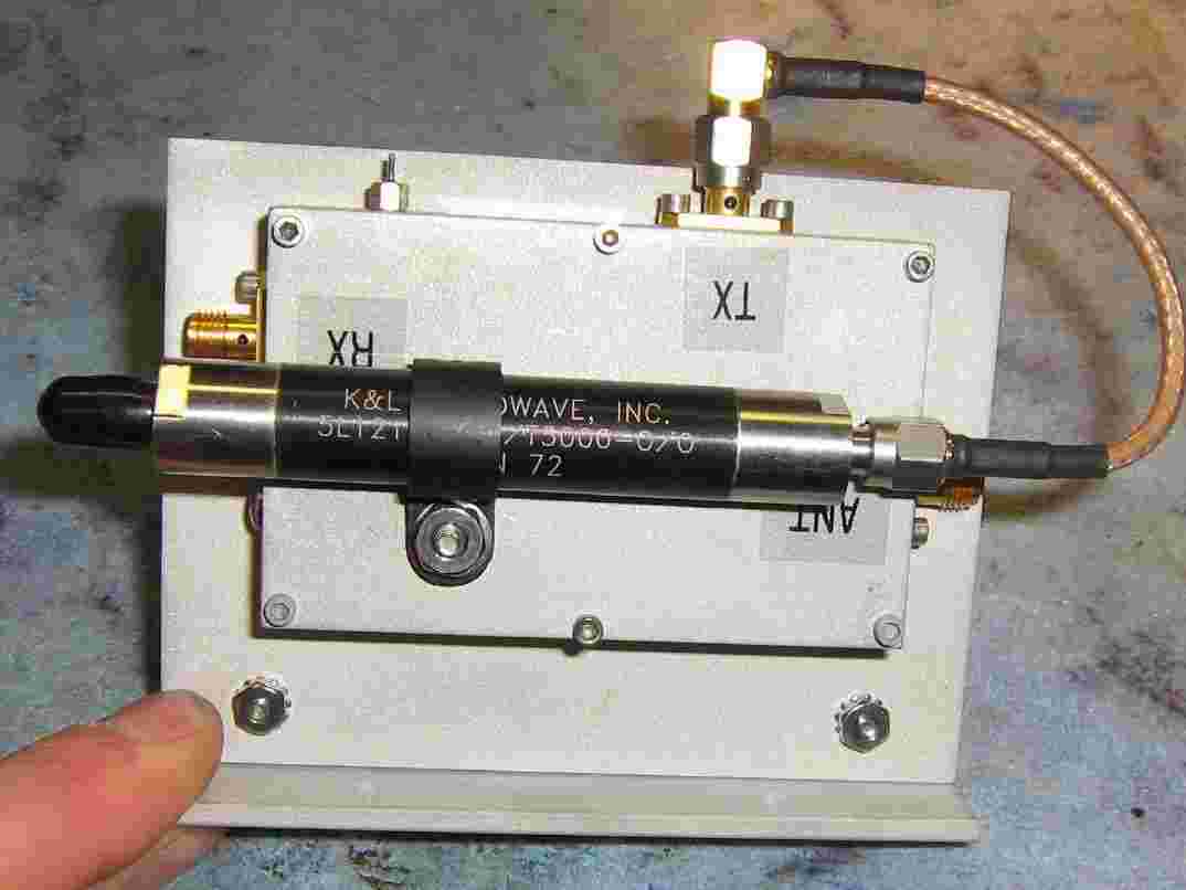
A high-quality external low-pass filter (or two) is required on the transmit port.
A K&L Microwave 5L121-1000/T5000-0/0 is shown above. The Mini-Circuits SLP-1000 is an equivalent.
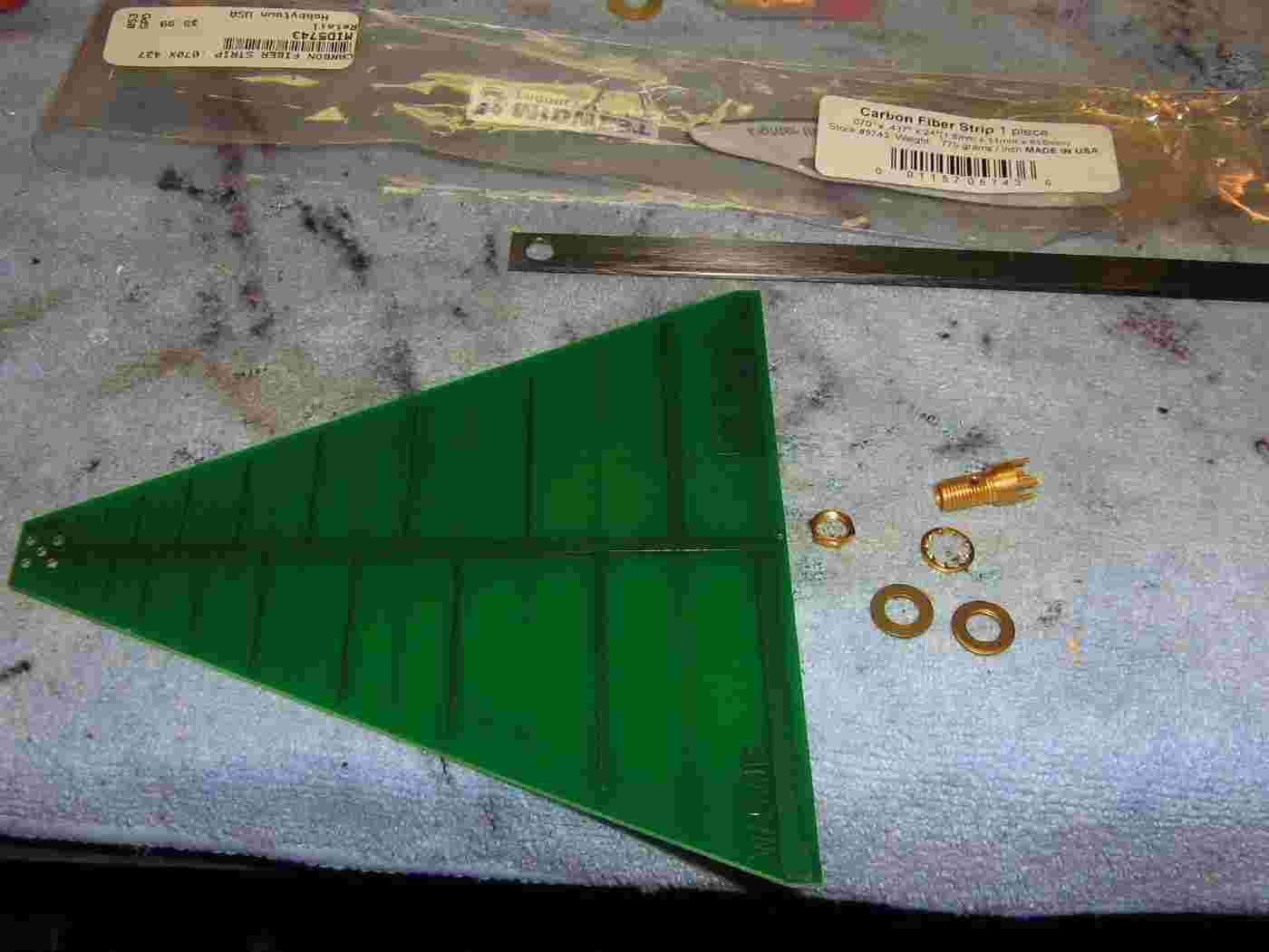
WA5VJB 850-6500 MHz log periodic antenna.
The diplexer allows the use of a single antenna for both transmitting and receiving. Since this will be a fairly wide frequency range, we'll need to a log periodic antenna.
Circular polarized antennas are recommended for non-linear junction detectors as the re-radiated signal from a proper non-linear junction will have the same polarity as the transmitted signal, while reflections from nearby objects will have the polarity "reversed." That provides an additional 20 dB isolation between the target and false signals. Unfortunately, homebrewing circulator polarized antennas for these frequencies can be quite difficult.
The WA5VJB 850-6500 MHz log periodic antenna has solder pads for installing a SMA connector and it is recommended you do this. A vertical panel-mount SMA connector is used here.
The log periodic antenna was then mounted to a short carbon fiber boom.
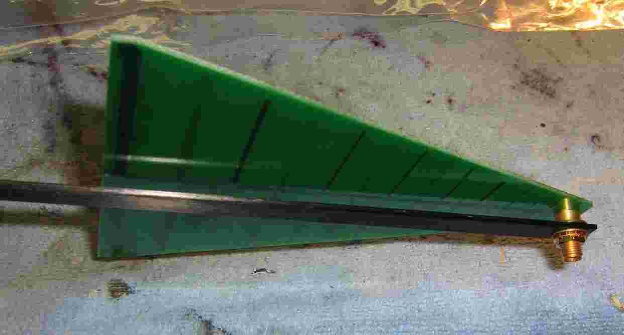
Overview of the semi-finished log periodic antenna.
Still trying to develop some type of additional mounting system. Real non-linear junction detectors have their antennas mounted on booms in order to scan hard-to-reach areas.
It should also be possible to easily change the non-linear junction detector's antenna polarization. After scanning an area with a vertical polarized antenna, switch to horizontal polarization and re-scan just be sure you didn't miss anything.
It's also possible to use two separate antennas for transmitting and receiving. This tends to provide the highest isolation and is the easiest setup when using higher RF illumination power.
These antennas are also very handy for other SIGINT applications so you may want to keep them portable.
Refer to the National LMX2316 datasheet for a more detailed explanation of the latches.
The Z-Comm PSN0930A is designed to be run in normal mode only. The FastLock options are not usable.
The latches should be loaded in this order: Initialization Latch, Function Latch, R Counter, and N Counter.
The "Initialization Latch" really isn't required, but it's listed in the datasheet so load it anyway.
All the latches are programmed as a 21-bit shift register with the Most Significant Bit (MSB) first and on the rising edge of the clock signal. Place the required value ("1" or "0") on the PSN0930A's Data line then bring the Clock line high then back low. Load the final 21-bit value into the PLL's latch by bringing the Load Enable line high then low. All this can be accomplished by using the SHIFTOUT command on the BASIC Stamp.
Function and Intialization Latches
MSB                                                                   LSB
F19 F18 F17 F16 F15 F14 F13 F12 F11 F10 F9 F8 F7 F6 F5 F4 F3 F2 F1 C2 C1
0   0   0   0   0   0   0   0   0   0   0  0  0  1  0  0  1  0  0  1  0
|
- C1, C2: Control Bits Should be "1 1" for Initialization Latch intialization.
- C1, C2: Control Bits Should be "0 1" for Function Latch intialization.
- F1: Counter Reset Should be "0" for normal operation.
- F2, F18: Power Down Should be "0" for normal operation.
- F3-F5: Lock Detect Modes Should be "1 0 0" for digital lock detect.
- F6: Phase Detector Polarity Should be "1" for Z-Comm synthesizers.
- F7: Charge Pump Tri-State Should be "0" for normal operation.
- F8-F17: Fast Lock & Test Modes All these bits should be set to "0" for normal operation.
- F19: Test Mode Should be "0" for normal operation.
R Counter
Since the Z-Comm PSN0930A will be using a 10 MHz reference frequency and the step size needs to be 100 kHz, the "R Counter" will be 100.
This means the "64," "32," and "4" bit divider ratios should be set to "1".
MSB                                                                   LSB
R19 R18 R17 R16 R15 R14 R13 R12 R11 R10 R9 R8 R7 R6 R5 R4 R3 R2 R1 C2 C1
0   0   0   0   0   0   0   0   0   0   0  0  1  1  0  0  1  0  0  0  0

                    8   4   2   1   5   2  1  6  3  1  8  4  2  1
		    1   0   0   0   1   5  2  4  2  6
		    9   9   4   2   2   6  8
		    2   6   8   4
|
- C1, C2: Control Bits Should be "0 0" for R Counter intialization.
- R1-R14: Divide Ratio This counter must be between 3 & 16,383.
- R15-R18: Test Mode Should be "0" for normal operation.
- R19: Lock Detect Precision Number of cycles to use for PLL lock detect.
N Counter
This is the main divider ratio and swallow bit counter for the PLL. Since the transmit frequency will be 902.0 MHz, the "N Counter" will need to be 9020 (902 MHz divided by the 100 kHz step size). The LMX2316 PLL has an internal dual-modulus "divide-by-32" prescaler on its RF input, so the "N Counter" is actually divided into a separate "B Counter" and "A Counter." The "B counter" will be 281 (integer of 9020 divided by 32) and the "A counter" will be 28. This is the swallow counter value required to get 281 * 32 (8992) to equal 9020.
N = (32 * B) + A
B = div(N / 32)
A = N - (B * 32)
Where div(x) is defined as the integer portion and 32 is the prescaler value.
An example "N" value for the transmitter at 902.0 MHz: 9020 = (32 * 281) + 28
The "B Counter" will be 281. This means the "256," "16," "8," and "1" bit divider ratios should be set to "1".
The "A Counter" will be 28. This means the "16," "8," and "4" bit divider ratios should be set to "1".
MSB                                                                   LSB
N19 N18 N17 N16 N15 N14 N13 N12 N11 N10 N9 N8 N7 N6 N5 N4 N3 N2 N1 C2 C1
1   0   0   0   0   1   0   0   0   1   1  0  0  1  1  1  1  0  0  0  1

    4   2   1   5   2   1   6   3   1   8  4  2  1  1  8  4  2  1
    0   0   0   1   5   2   4   2   6               6
    9   4   2   2   6   8
    6   8   4
    <----------------B Counter------------------->  <-A Counter->
|
- C1, C2: Control Bits Should be "1 0" for N Counter intialization.
- N1-N5: A Counter This counter must be between 0 & 31.
- N6-N18: B Counter This counter must be between 3 & 8,191.
- N19: GO Bit Charge pump output current (1 mA). Should be "1" for Z-Comm synthesizers.
The BASIC Stamp SHIFTOUT command will be used to program the Z-Comm PSN0930A. Refer to the BASIC Stamp Syntax and Reference Manual for all the nitty-gritty details you'll need for the SHIFTOUT command.
SHIFTOUT, DataPin, ClockPin, Mode, [OutputData\Bits]
|
Where DataPin is the BASIC Stamp pin connected to the Z-Comm PSN0930A Data line and ClockPin is connected to the Z-Comm PSN0930A Clock line.
The Mode will be Most Significant Bit (MSB) first, which is common in these applications. This should be set to "1".
The [OutputData\Bits] is the complicated part, as the SHIFTOUT command only works 16 bits at a time and the LMX2316 in the Z-Comm PSN0930A requires a 21-bit latch.
We can overcome this by loading the data in two separate SHIFTOUT calls. One to load the first 16 bits then another to load only the last 5 bits. The Load Enable line can be controlled using the normal HIGH and LOW BASIC Stamp commands.
Refer to the Analog Devices ADF4106 datasheet for a more detailed explanation of the latches.
This device is quite similar to programming the PSN0930A except that the shift registers are 24 bits long and some bit values are a little different.
The latches should be loaded in this order: Initialization Latch, Function Latch, R Counter, and N Counter.
Function and Intialization Latches
MSB                                                                               LSB
F22 F21 F20 F19 F18 F17 F16 F15 F14 F13 F12 F11 F10 F9 F8 F7 F6 F5 F4 F3 F2 F1 C2 C1
1   0   0   1   1   1   1   1   1   0   0   0   0   0  0  0  0  0  0  1  0  0  1  1
|
- C1, C2: Control Bits Should be "1 1" for Initialization Latch intialization.
- C1, C2: Control Bits Should be "0 1" for Function Latch intialization.
- F1: Counter Reset Should be "0" for normal operation.
- F2, F20: Power Down Should be "0" for normal operation.
- F3-F5: Lock Detect Modes Should be "1 0 0" for digital lock detect.
- F6: Phase Detector Polarity Should be "0" for Mini-Circuits synthesizers.
- F7: Charge Pump Tri-State Should be "0" for normal operation.
- F8, F9: FastLock Should be "0 0" for normal operation.
- F10-F13: Timer Counter Should be "0 0 0 0" for normal operation.
- F14-F19: Charge Pump Current Setting Should be "1 1 1 1 1 1" for Mini-Circuits synthesizers.
- F21-F22: Prescaler Should be "0 1" for divide-by-32.
R Counter
Since the Mini-Circuits DSN-2300A-1119 will be using a 10 MHz reference frequency and the step size needs to 250 kHz, the "R Counter" will be 40.
This means the "32" and "8" bit divider ratios should be set to "1".
MSB                                                                               LSB
R22 R21 R20 R19 R18 R17 R16 R15 R14 R13 R12 R11 R10 R9 R8 R7 R6 R5 R4 R3 R2 R1 C2 C1
0   0   0   0   0   0   0   0   0   0   0   0   0   0  0  0  1  0  1  0  0  0  0  0

                                8   4   2   1   5   2  1  6  3  1  8  4  2  1
                                1   0   0   0   1   5  2  4  2  6
                                9   9   4   2   2   6  8
                                2   6   8   4
|
- C1, C2: Control Bits Should be "0 0" for R Counter intialization.
- R1-R14: Divide Ratio This counter must be between 3 & 16,383.
- R15, R16: Anti-Backlash Should be "0 0" for normal operation.
- R17, R18: Test Mode Should be "0 0" for normal operation.
- R19: Lock Detect Precision Number of cycles to use for PLL lock detect.
- R20-R22: Not Used Should be "0 0 0" for normal operation.
N Counter
This is the main divider ratio and swallow bit counter for the PLL. Since the local oscillator frequency will be 2240 and 2270 MHz, the "N Counter" will need to switch between 8960 (2240 MHz divided by the 250 kHz step size) and 9080. The ADF4106 will be programmed to use a dual-modulus "divide-by-32" prescaler on its RF input.
The "B counter" for generating 2240 MHz will be 280 (integer of 8960 divided by 32) and the "A counter" will be 0. The "B counter" for generating 2270 MHz will be 283 (integer of 9080 divided by 32) and the "A counter" will be 24.
You can change the N counter "on the fly" after the other latches are all programmed.
N = (32 * B) + A
B = div(N / 32)
A = N - (B * 32)
Where div(x) is defined as the integer portion and 32 is the prescaler value.
An example "N" value for the oscillator at 2240 MHz: 8960 = (32 * 280) + 0
An example "N" value for the oscillator at 2270 MHz: 9080 = (32 * 283) + 24
For 2240 MHz, the "B Counter" will be 280. This means the "256," "16," and "8" bit divider ratios should be set to "1". The "A Counter" will be 0. This means all the bit divider ratios should be set to "0".
For 2270 MHz, the "B Counter" will be 283. This means the "256," "16," "8," "2," and "1" bit divider ratios should be set to "1". The "A Counter" will be 24. This means the "16," and "8" bit divider ratios should be set to "1".
MSB   For 2240 MHz                                                                LSB
N22 N21 N20 N19 N18 N17 N16 N15 N14 N13 N12 N11 N10 N9 N8 N7 N6 N5 N4 N3 N2 N1 C2 C1
0   0   1   0   0   0   0   1   0   0   0   1   1   0  0  0  0  0  0  0  0  0  0  1

            4   2   1   5   2   1   6   3   1   8   4  2  1  3  1  8  4  2  1
            0   0   0   1   5   2   4   2   6                2  6
            9   4   2   2   6   8
            6   8   4
            <-----------------B Counter------------------->  <--A Counter--->
|
- C1, C2: Control Bits Should be "1 0" for N Counter intialization.
- N1-N6: A Counter This counter must be between 0 & 63.
- N7-N19: B Counter This counter must be between 3 & 8,191.
- N20: Charge Pump Gain Should be "1" for Mini-Circuits synthesizers.
- N21-N22: Not Used Should be "0 0" for normal operation.