For this amplifier project, we'll being using an external Astec ACV-15N3 +15 VDC, 3A power supply.
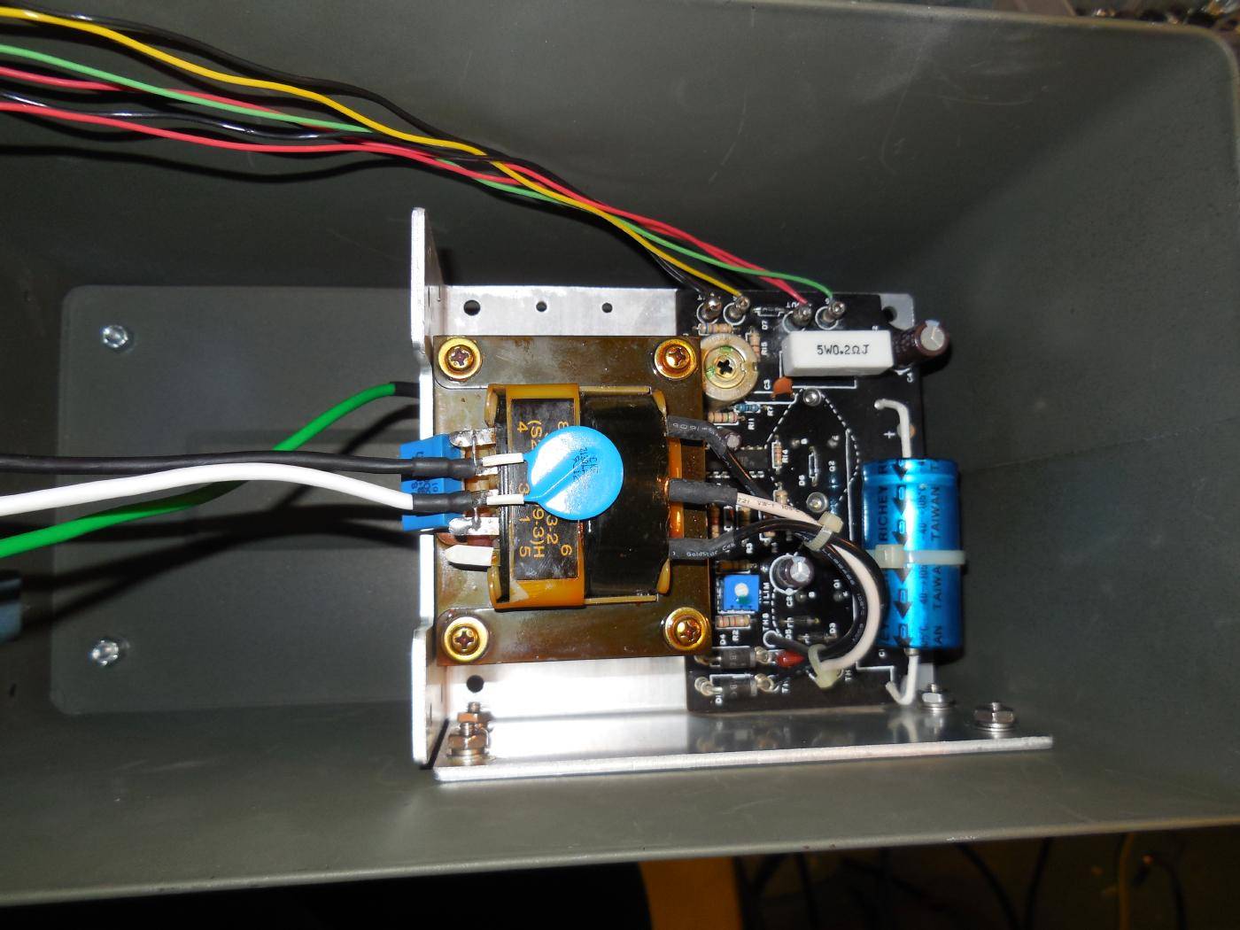
The blue disk on the primary is a 150 VAC Metal-Oxide Varistor (MOV) to protect against any voltage transients on the incoming AC mains.
The blue rectangle device on the primary is an optional "snubber." This device consists of a series 120 ohm / 0.033 µF AC-rated capacitor to prevent the generation of a large voltage spike when power is turned off.
The Astec ACV-15N3 power supply has four output terminals: +15 VDC Output, +15 VDC Return (Ground), Sense +, and Sense -.
The power supply will be built into an old ammo can.

Overview of the incoming AC mains components.
The 120 VAC mains input is via a standard filtered IEC connector.
The black "hot/live" lead then passes through a panel-mounted 15 amp circuit breaker.
It then goes to a SPST switch for power control.
The white wire is the AC mains "neutral." The green wire is the AC mains Earth ground.
Three optional ferrite beads are on each of the AC mains wires right after the IEC connector to help knock down any incoming EMI on the power line.
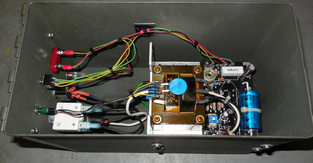
Internal overview of the completed +15 VDC, 3A power supply.
There is a DPST switch to select either internal or external sense for the power supply. This is optional, but highly recommended if your power supply supports it.
There is a green neon lamp for a "power on" indicator.

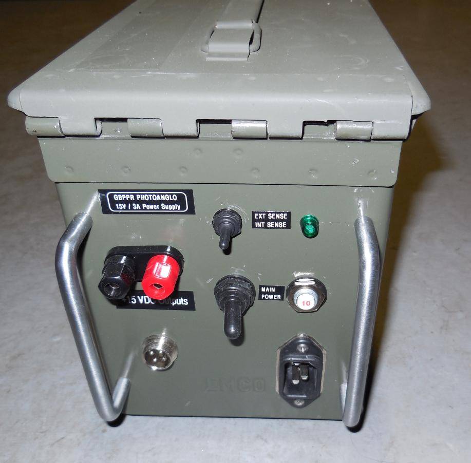
Front-panel overview of the completed +15 VDC, 3A power supply.
A 4-pin microphone jack is used for the main +15 VDC output and the sense connections.
Pin      Description                Wire Color
1        +15 VDC Output             Red
2        +15 VDC Return / Ground    Black
3        Sense -                    Green
4        Sense +                    White
The banana jacks are for an extra +15 VDC output. This is optional, but could be useful for powering other projects.
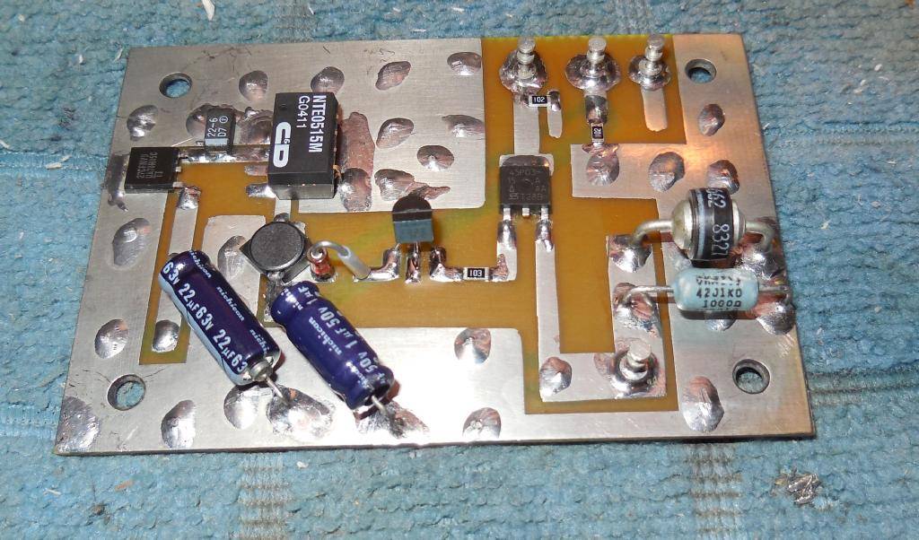
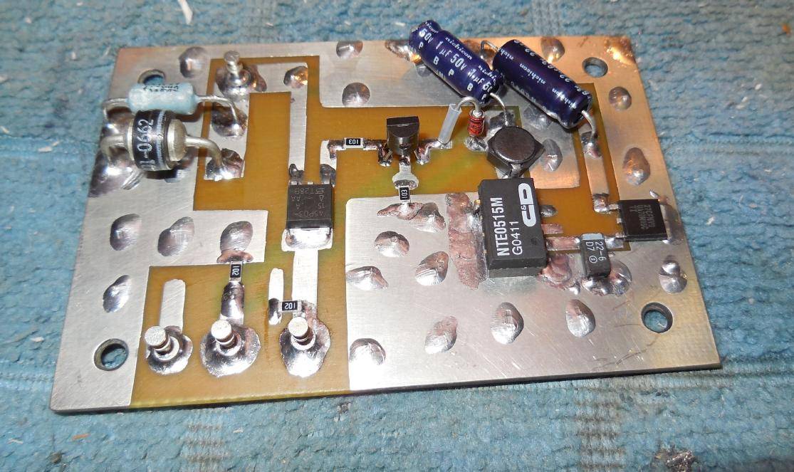
Overview of the -15 VDC negative voltage generator and sequencer circuit board.
The main +15 VDC input is via the solder terminal on the lower-right. It is regulated down to +5 VDC to power the Murata NTE0515M DC-to-DC converter, which is the black box on the upper-left.
The -15 VDC output is tapped to control a sequencer circuit consisting of a 1N4743 13V Zener diode, 2N2222A transistor, and Vishay SUD45P03 P-channel MOSFET.
This circuit holds off applying the +15 VDC main line to the amplifier before the -15 VDC bias is applied. This is required to prevent damaging the RF power amplifier.
Alternate view.
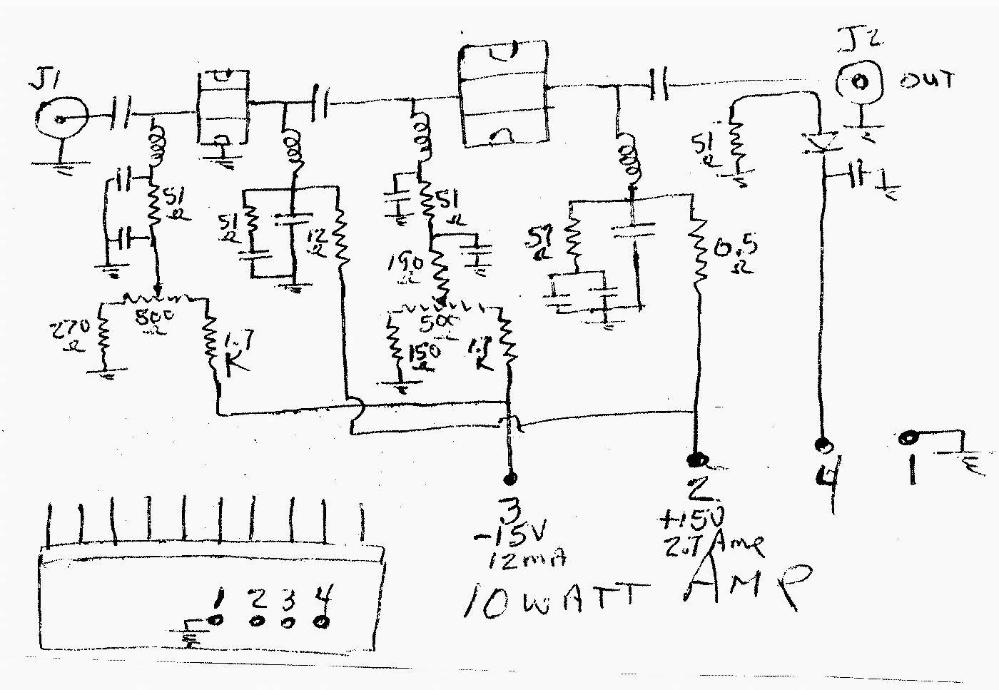
The three solder terminals along the bottom connect to the Comwave SB010 are the RF diode detector output, -15 VDC bias, and +15 VDC.

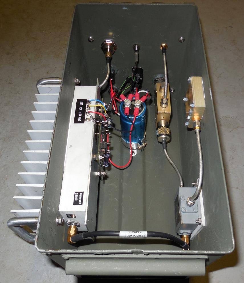
Internal view of the Comwave SB010 10 watt MMDS amplifier.
The RF input (+20 dBm / 100 mW) is on the right-side, RF output (+40 dBm / 10W) is on the left-side.
+/- 15 VDC power, ground, and the RF detector output are via the feed-through capacitors on the lower-left.
Terminal A is a common ground.
Terminal B is +15 VDC at around 2.7 amps.
Terminal C is -15 VDC at around 12 mA and must be applied first.
Terminal D is the DC output of the diode RF detector.
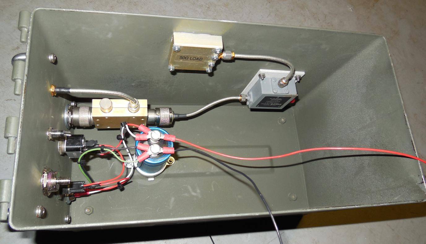
Mounting the Teledyne C-2S43A-1 ferrite circulator, EMC 50 ohm load, and Meca 715-20-2.5 directional coupler.
The optional ferrite circulator will protect the amplifier in case of a SWR mismatch and the optional directional coupler is for sampling the output RF power or for driving the local oscillator port on an external mixer.
The is a large 4,700 µF / 50V capacitor on the +15 VDC input (red) to the case.
The negative terminal of this capacitor is used as a single-point ground.
The Sense + (white) and Sense - (green) connections are also to the terminals on this capacitor.
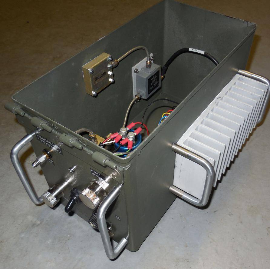
The stock finned heatsink on the Comwave SB010 was removed and holes where drilled in the case so the body of amplifier can be mounted internally and the heatsink externally.
The amplifier does get fairly warm, but it's not excessive and shouldn't require a fan.
Brass drawer handles prevent the heatsink from being damaged.
Make sure there is a large - but thin - layer of heatsink grease between the amplifier's body, the case, and the heatsink.
Completed amplifier case overview.
RF input to the amplifier is via the N female connector on the upper-left.
The final RF output from the Meca directional coupler goes to a panel-mount N connector.
The 20 dB tap from the directional coupler goes to a panel-mount SMA connector.
All the RF connections should be made using semi-rigid or conformable coax for maximum RF isolation.

Completed amplifier front-panel overview.
The input from the external +15 VDC power supply is on the lower-right via the 4-pin microphone jack.
There is also a 5A fuse and SPST power switch on the +15 VDC input.
10 watt RF output is via the bottom N connector.
The +20 dBm (100 mA) RF input is via the upper-right N connector.
20 dB tap from the directional coupler is via the SMA connector. There should be a 50 ohm load installed when not in use.
There is a green LED for a "power on" indicator.