- Introduction
- Receiver
- Transmitter (format PDF)
- Photos
- Opis działania projektu transmisji z widmem rozproszonym
- Nadajnik
- Odbiornik
- Zdjęcia
Voice link over spread spectrum radio
Transmisja dźwięku z wykorzystaniem widma rozproszonego.
|
|
|
How to receive signal Signal with spread spectrum has pseudo-noise character
and large spectrum. Using normal receiver even with ten same frequency
band, we receive only higher noise level, no signal. It is impossible
to try manually find any station. The receiver for spresd spectrum systems
is much more complicated than narrow-band receiver.
Synchronization The most difficult problem in Spread Spectrum systems is synchronization of PN sequences in transmitter and receiver (d.). Only when PN sequences in receiver and transmitter have the same phase, it is possible to despread spectrum of signal. (spectrum of signal was spread in transmitter). We have some options:
In other method (b.) frequencies of PN generators in receiver and transmitter are synchronized by other external signals. We can use local MW broadcast radio, TV synchro-signals, or DCF77 or other. In this case we must manually adjust phase of PN sequence (once at beginning of transmission). Transmitter and receiver must have modules for receive external signals. The most critical and most difficult is method (c.), without additional signals. In this case transmitter is less complicated, and receiver is most complicated. Receiver must receive right frequency, and must find moment of synchronization, fine adjust frequency of PN generator, hold phase of PN sequence, When phases of PN sequences in transmitter and receiver are different more than ½ byte (too early or to late), synchronization circuit must correct frequency of PN generator (decrease or increase). We adjust crystal generators in transmitter and receiver to the same frequency, but their frequencies are little difference. It is why phase of PN sequence in receiver is changing (compare to transmitter). Every some seconds (time depends on difference in frequencies) we have identical phases of PN sequences. In this moments spectrum of received signal is despreaded. On output of receiver we have higher level of signal (impulse). This impulses we use to find moments of synchronization. |
How to hold right phase
We need 2 information about phase of PN sequence in receiver:
Receiver block diagram description
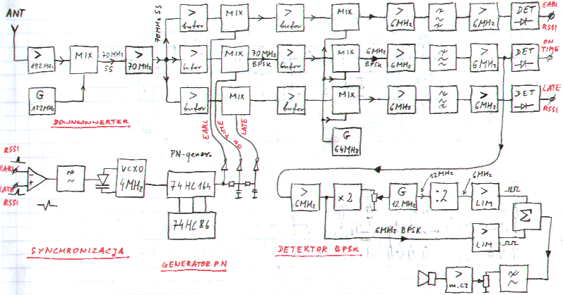
Fig.1
Incoming wideband signal 192MHz with spread spectrum from antenna goes to input amplifier. This amplifier must have bandwidth more than 8MHz. We can control gain of this amplifier by changing voltage on second gates of T1 and T2. Amplified signal is downconverted by mixer UL1042 (SO42P). Mixer is driven by first local oscillator 122MHz. The product of mixer we need is wideband first IF 70MHz (192-122). First IF has spread spectrum from about 66MHz to 74MHz. IF amplifier must have bandwidth more than 8MHz. Amplified first IF is split to 3 identical branches. In each sighal branch (EARLY, ON-TIME, LATE) signal with spread spectrum after buffer goes to double balanced mixer configured as biphase shift keyer. Mixers (DBM) in signal branches are driven by PN sequences (identical as in transmitter) shifted about ½ byte. (EARLY-PN, ON-TIME-PN, LATE-PN). If PN sequence has identical phase as PN sequence in transmitter (synchronism), spectrum of signal will be despreaded. In this case from mixer to buffer goes narrowband signal 70MHz. It is phase-modulated BPSK signal. Narrowband signal 70MHz goes to next mixer (downconverter) made of 2-gate FET T3. The lower gates of FET-transistors are driven by second local oscillator 64MHz. The product of mixer we need is narrowband signal (second IF) 6MHz. It is phase-modulated BPSK signal. After filter and amplifier signal goes to AM detector. Output voltage of AM detectors depends on incoming signal RSSI. (only in case of synchronism). When PN sequence in receiver has the same phase as PN sequence in transmitter, we have ON-TIME-RSSI which signal we can use to signal indicator (not showed). When PN sequence in receiver is earlier about ½ byte than PN sequence in transmitter, we have EARLY-RSSI signal, which is used to decrease frequency of 4 MHz oscillator. When PN sequence in receiver is later about ½ byte than PN sequence in transmitter, we have LATE-RSSI signal, which is used to increase frequency of 4MHz oscillator. Both impulses EARLY-RSSI and LATE-RSSI are used to synchronization of 4MHz oscillator, which drives PN generator (identical as one in transmitter). The PN generator is made of shift register 74HC164 and EX-OR gates 74HC86. PN sequence is 2 times delayed about ½ byte and buffered by 74HC14 gates. We have 3 PN sequences (identical as one in transmitter), but delayed about +½ byte and -½ byte. This 3 PN sequences (EARLY-PN, ON-TIME-PN, LATE-PN) drive despreading mixers in 3 signal branches (EARLY, ON-TIME, LATE). Narrowband signal from ON-TIME branch goes to BPSK demodulator. Signal is amplified by 6MHz amplifier and is multiplied x2 to 12MHz. Signal 12MHz is used to synchronize 12MHz generator. Sinus 12MHz from this generator goes to divider by 2. We have 6MHz signal with constant phase. Two signals: from divider and from 6MHz amplifier after amplifier and limiter are sumed. When their phases are the same, we have "1". When their phases are different, we have "0". As digital to analog converter is used low-pass filter. Analog audio signal after amplifier goes to speaker.
Detailed description of receiver.
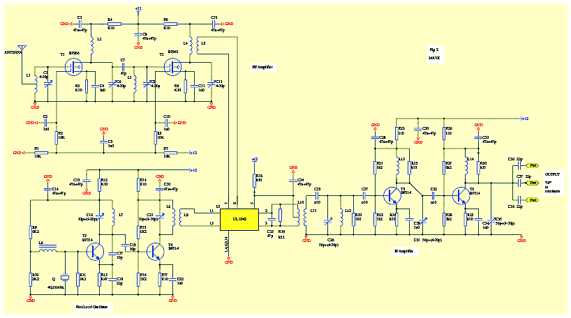
Fig.2 (PDF format)
Incoming from antenna wideband signal 192MHz with spread spectrum goes to input amplifier (fig.2). This amplifier must have bandwidth more than 8MHz. We can control gain of this amplifier by changing voltage on second gates of T1 and T2 (AGC circuit not showed). Amplified signal is downconverted by mixer UL1042 (SO42P). Mixer is driven by first local oscillator 122MHz. The best is circuit without frequency multiplier. In our generator with T3 (taken from narrowband receiver) we use crystal Q=40,68MHz and multiplier x3 and buffer 122MHz with T4. However second harmonic (about 81,4MHz) can pass through first IF amplifier. It is why first local oscillator (with T3) and buffer (with T4) must be shielded. But better solution is to use crystal Q=122MHz. The product of mixer we need is wideband first IF 70MHz (192-122). First IF has spread spectrum from about 66MHz to 74MHz. IF amplifier must have bandwidth more than 8MHz. In our first IF amplifier (taken from narrowband receiver), to make bandwidth wider we add resistors parallel to LC circuits in collectors of T5 and T6. This IF amplifier is temporary solution. LC circuits with parallel resistors decrease amplification. Flat characteristic of our IF amplifier includes second harmonic of crystal oscillator (about 81,4MHz). Under construction is new wersion of IF amplifier with band-pass filters. Amplified first IF goes to correlator (showed on fig.3), where is split to 3 identical branches.
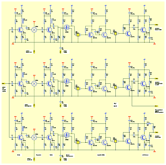
Fig. 3 (PDF format)
Amplified first IF is split to 3 identical branches (fig.3). In each sighal branch (EARLY, ON-TIME, LATE) signal 70 MHz with spread spectrum is buffered by T1 and goes to double balanced mixer configured as biphase shift keyer. Mixers (DBM) in signal branches are driven by PN sequences (identical as in transmitter) shifted about ½ byte. (EARLY-PN, ON-TIME-PN, LATE-PN). If PN sequence has identical phase as PN sequence in transmitter (synchronism), spectrum of signal will be despreaded. In this case from mixer to buffer with T2 goes narrowband signal 70MHz. It is phase-modulated BPSK signal. Narrowband signal 70MHz goes to next mixer (second downconverter) made of 2-gate FET T3. The lower gates of FET-transistors are driven by second local oscillator 64MHz. The product of mixer we need is narrowband signal (second IF) 6MHz. It is phase-modulated BPSK signal.From the drain of T3 signal goes to 6 MHz filter with bandwidth about 200kHz. Next, signal is amplified by 2-stage amplifier with T4, T5. After second 6Mhz filter and last amplifier with T6 signal goes to AM detector made of T7. On it's output (emmiter of T7) voltage level depends on incoming signal RSSI. (only in case of synchronism). Because of low level of voltage on emmiter of T7 (less than 1V), divider 10k/10k is added. On it's output voltage is about 1 of power supply voltage. When no signal is incoming, we should have almost identical levels of voltage on outputs of LATE-branch and EARLY-branch. It is why in LATE branch in divider 10k/10k in place of one resistor 10k there is 8k2 resistor and 6k8 variable resistor. With this variable resistor we can equalise levels of EARLY-RSSI and LATE-RSSI (adjust when no signal is inciming). Even when we have no incoming signal, on outputs of each 3 branches we have quite high level of voltage (quite high RSSI signals). It is because of noises and false products of mixers and their cobbinations. However in case of synchronism, despreaded spectrum of signal makes narrow-band signal and this narrow-band signal increases level of RSSI voltage. RSSI-LATE and RSSI-EARLY impulses goes to sinchronization circuit (showed on fig.4). This circuit controls 4MHz VCXO (showed on fig.4) for PN generator. When ON-TIME-PN sequence has identical phase than PN sequence in transmitter, on the output of ON-TIME branch we have RSSI-ON-TIME. This signal we can use to indicate level of RF signal incoming to antenna. We can also use RSSI-ON-TIME in AGC loop (not showed). In this branch ON-TIME before AM detector we have amplified 6MHz BPSK modulated signal, carrying infofmation. This signal goes to BPSK demodulator (showed on fig.5).
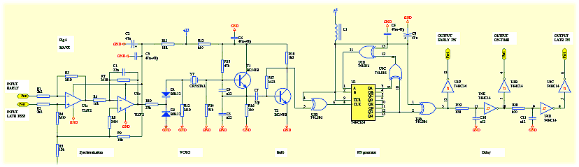
Fig.4 (PDF Format)
The PN generator in receiver (fig.4) is identical as PN generator in transmitter. It is made of shift register 74HC164 and EX-OR gates 74HC86 in feed-back circuit. We use 7 registers. It allows to generate PN code of 127 bytes length. The PN sequence is 2 times delayed about 1/2 byte. To delay we use 2 RC circuits (k33 and n22). So on the outputs we have 3 identical PN sequencies but with different phases. EARLY-PN sequence is earlier about 1/2 byte, and LATE-PN sequence is laterer about 1/2 byte, compare to ON-TIME-PN sequence. Unlike in transmitter, in receiver PN generator is driven by 4MHz VCXO. In receiver we can not use normal 4MHz crystal oscillator. VCXO must keep absolutely the same frequency and the same phase than oscillator in transmitter. VCXO is made of T1 and buffer with T2. Oscillator is stabilized by crystal 4MHz and tuned by 2 varicaps BB112. Tuning range is about 3999500-4000500 Hz. The DLL circuit contains 2 operational amplifiers. RSSI-LATE impulses from LATE branch (showed on fig.3) go to non-inverting input of first opamp. After amplifing and filtering this impulses are used to increase of frequency of VCXO. RSSI-EARLY impulses from EARLY branch (showed on fig.3) go to inverting input of first opamp. After amplifing and filtering this impulses are used to decrease of frequency of VCXO. On the output of first opamp in case of no incoming signal or in case of synchronism, we have voltage level about 3V (adjusted by variable resistor 6k8 in LATE branch). In normal operation (synchronism) impulses higher than 3V appear when frequency of VCXO is too high and it is nesesery to slow down, or impulses lower than 3V appear when frequency of VCXO is too low and it is nesesery to hurry up. Second opamp is used as low pass filter and it amplifies impulses to amplitude about 5V (to ensure wide tuning range: +/-0.5kHz). Amplified impulses go to varicape diodes in VCXO to control frequency.
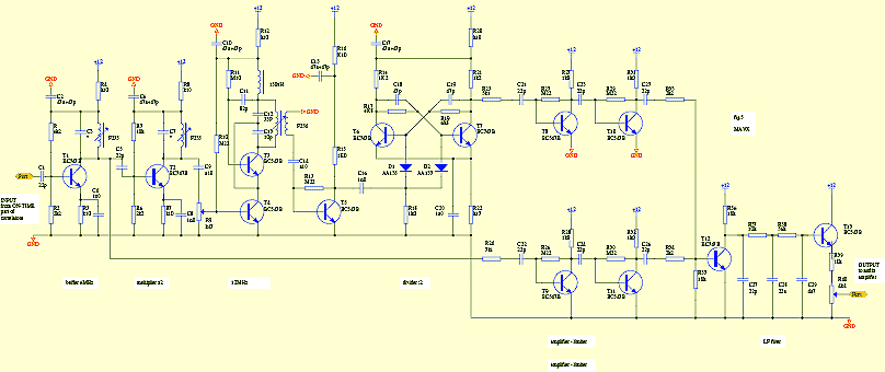
Fig. 5 (PDF format)
Narrowband signal from the middle branch of correlators ON-TIME (fig. 3) goes to BPSK demodulator (fig. 5). Signal is amplified by 6MHz amplifier with T1 and is multiplied x2 to 12MHz by multiplier with T2. Multiplied signal has constant phase, but its envelope is deformed, his amplitude has fadings. Signal 12MHz is used to synchronize 12MHz generator made of T3, T4. Sinus 12MHz from this generator is amplified by T5. Amplified signal 12MHz goes to divider by 2 with trigger made of T6, T7. After amplifier and limiter with T8, T9 we have 6MHz square signal with constant phase which is used as pattern signal. Incoming BPSK signal amplified by T1 is additional amplified and limited by T10, T11. This signal is sumed with pattern 6MHz signal on R 10k. When their phases are the same, amplitude on R 10k increases. Wheh phases of both 6MHz signals are different, amplitude on R 10k decreases. After amplitude detector with T12 we have "1" or "0" depend phase of BPSK signal. This is digital audio signal equivalent to digital audio signal in transmitter. The output of BPSK demodulator does not recover original data polarity. We receive stream of bits identical or inverted compare to original digitalized voice stream in transmitter. In long time transmission, the polarity of digital signal can change a few times, because of fadings or disturbations of work of BPSK demodulator. Because as a digital to analog (D/A) converter we use integrator and low-pass filter, change of polarity of digital signal from BPSK demodulator causes only change phase of audio output signal. We can not hear it. It is why the polarity recover is no needed in receiver. Analog audio signal from R 4k7 goes to amplifier (fig. 6).
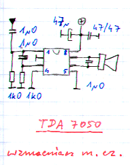
Fig. 6 |
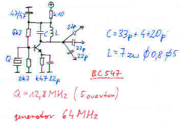
Fig . 7 |
Output audio amplifier (fig. 6) is made of TDA7050. Circuit is conventional, working from Ucc=3V. Be sure than both wires to loudspeker are isolated from GND.
The 64MHz oscillator (second heterodyne) is made using harmonic frequency of crystal (fig. 7). The crystal works on 5-th overtone. Parallel LC circuit in collector of transistor, we adjust for maximum output signal 64MHz. Sine signal 64MHz goes to lower gates of FETs in each of 3 branches of correlators (fig. 3).
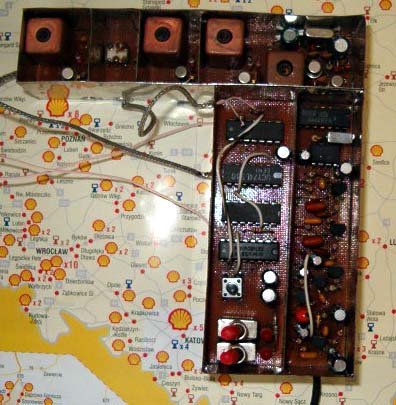
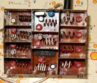
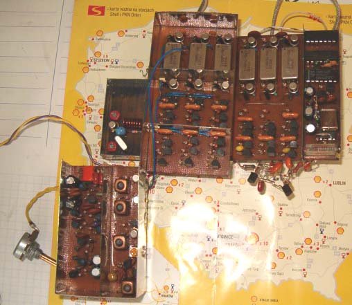
Photos |
Click on thumbnail to see pictures | |
Transmitter
|
Downconverter
|
Receiver
|
| Author: Walery
Maksymiuk 2002-10.11.2005 |
Edycja i opracowanie HTLM: SP4IZK