While not the most electrically complicated section of a radar system, the pulse modulator is the one section I am not really sure about, and should still be considered very experimental.
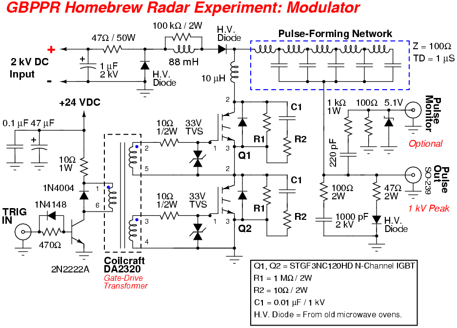
The pulse modulator is essentially a system which charges a Pulse-Forming Network (PFN) up to a certain high-voltage, 2 kV in our case, and then quickly "grounds" the PFN's positive terminal through the primary winding on an external pulse transformer. This is done using some type of controllable high-speed switch, usually a hydrogen thyratron tube. The generated high-voltage pulse is what is eventually used to "fire" the magnetron, causing it to emit a RF pulse equal to the PFN's delay time, 1 µS for our example.
Most commercial radars use a high-voltage thyratron trigger (5C22) or even spark gaps to rapidly discharge the PFN, but thyratrons are getting to be difficult to locate and can be quite expensive. For our modulator, we'll be using common high-voltage Insulated Gate Bipolar Transistors (IGBT), which are available from places like Mouser or Digi-Key for only a few dollars a piece. Two IGBTs will need to be used in series to equal the required stand-off operating voltage (2,000 volts) for our modulator. Single high-voltage IGBTs or IGBT blocks are available, and would be much easier to work with, but are still very expensive. A gate-drive transformer will be required to trigger both the IGBTs at the same time and to also provide the proper high-voltage isolation. Because of the voltage difference across the two IGBTs, you won't be able to use a single gate-drive circuit with a common ground.
The proper IGBT gate-drive circuit is the part of the system I had the most trouble with, and what is shown should be considered just a starting point. The key is getting the two IGBTs to fire at the same time - when you want them to - and with the proper high-voltage isolation. From experience, the two series transistors will require parallel resistors to "share" the voltage load across each of them so the transistor with the lowest leakage current won't be forced into avalanche mode, which can destroy it. Series resistor/capacitor snubbers will also be added across the transistors to help protect the transistors from transients if they both don't switch on time.
The IGBTs used here (ST Electronics STGF3NC120HD N-channel, 3A/1,200V) have an internal damper diode. These internal diodes will serve an important purpose for our radar application. If the impedance of the PFN and the pulse transformer's primary are not matched, a residual voltage charge can be left on the PFN during the dischage cycle. This residual voltage charge can distort the overall shape of next pulses or can even cause the magnetron to misfire or change frequency. The "reverse diode" in the IGBT will help to completely discharge the PFN after each pulse, thus allowing the PFN to be recharge to the same voltage potential for each pulse.
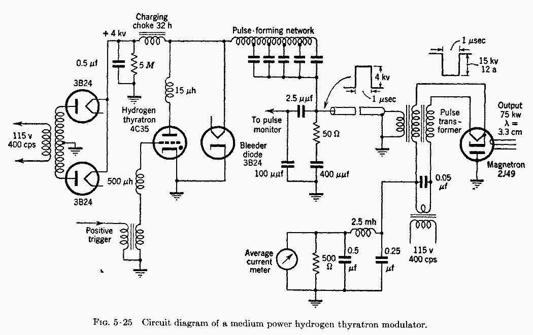
A real radar pulse modulator uses a "resonant" inductor/capacitor circuit to charge the PFN. A large inductor is added in series with the PFN charging line to resonate with the overall capacitance of the PFN at half the operating pulse frequency. The idea is to "add" the inductor's stored DC high-voltage charge onto the PFN's voltage. This is done because a PFN circuit outputs only half of its charging voltage, and this is a simple trick to get a voltage boost without requiring any more costly windings on the magnetron's pulse transformer secondary. Because of the low PFN operating frequency, the required value of this series charging inductor can be very high. A five henry inductor would be required for the circuit we're building here, assuming a 2,000 Hz Pulse-Repetition Frequency (PRF). Some commercial radars have charging inductors with values of 30 henries or more. We'll just be using a series 88 mH torroid inductor (mostly as a RF choke) to protect the high-voltage power supply from induced spikes. The series charging diode also protects the power supply during the discharge cycle and allows for changing the modulator's pulse-repetition frequency when using a resonant DC charging network.

Overview of the pulse modulator's high-voltage DC input to the ammo box we'll be using for the project's case.
The input is via a pair of insulated banana jacks.
The 1 µF / 2 kV capacitor is from an old microwave oven. The protection high-voltage diode is also from an old microwave oven. Note one of the capacitor's terminals is used as a common ground point which is then connected to the metal project case.
The high-power series 47 ohm resistor is probably optional, but will help to protect the high-voltage power supply in case anything short circuits.
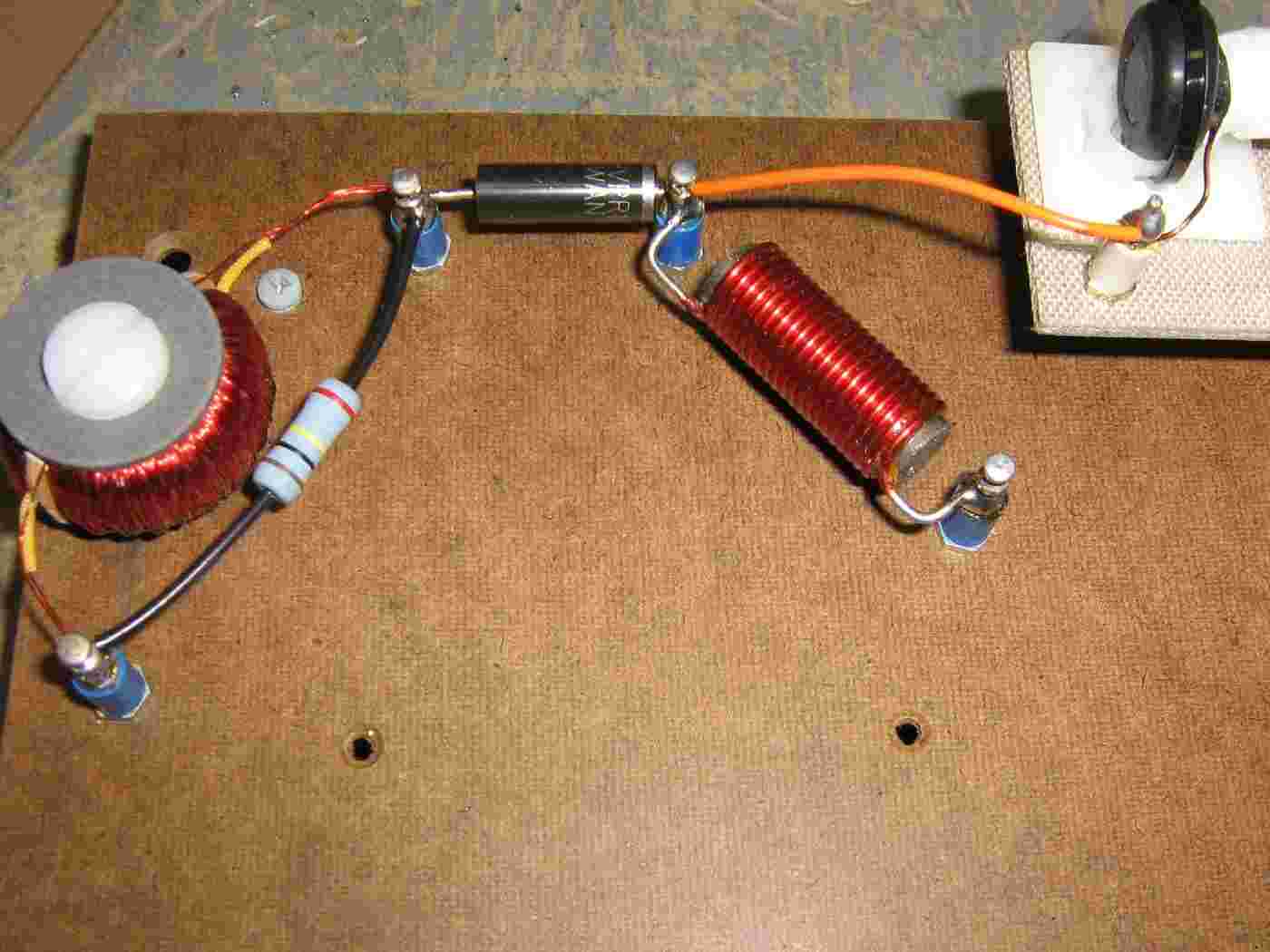
Overview of the PFN charging network.
The positive 2 kV DC input comes in on the solder terminal on the lower-left.
The 88 mH charging inductor is the big red donut on the left. A 100 kohm parallel resistor is used to "de-Q" the inductor. Not sure if that resistor is required or not.
The series high-voltage diode is a HVPR16-06, or any voltage-doubler diode from an old microwave oven should work.
The large red coil on the right is a 10 µH inductor used to help tame the large current spike when the PFN discharges through the IGBTs, and is probably also optional.
The circuit board for this pulse modulator is built onto the fiberboard base from an old clipboard and most of the connections will be made using solder terminals. This is to help with high-voltage isolation and to make component changes much easier.
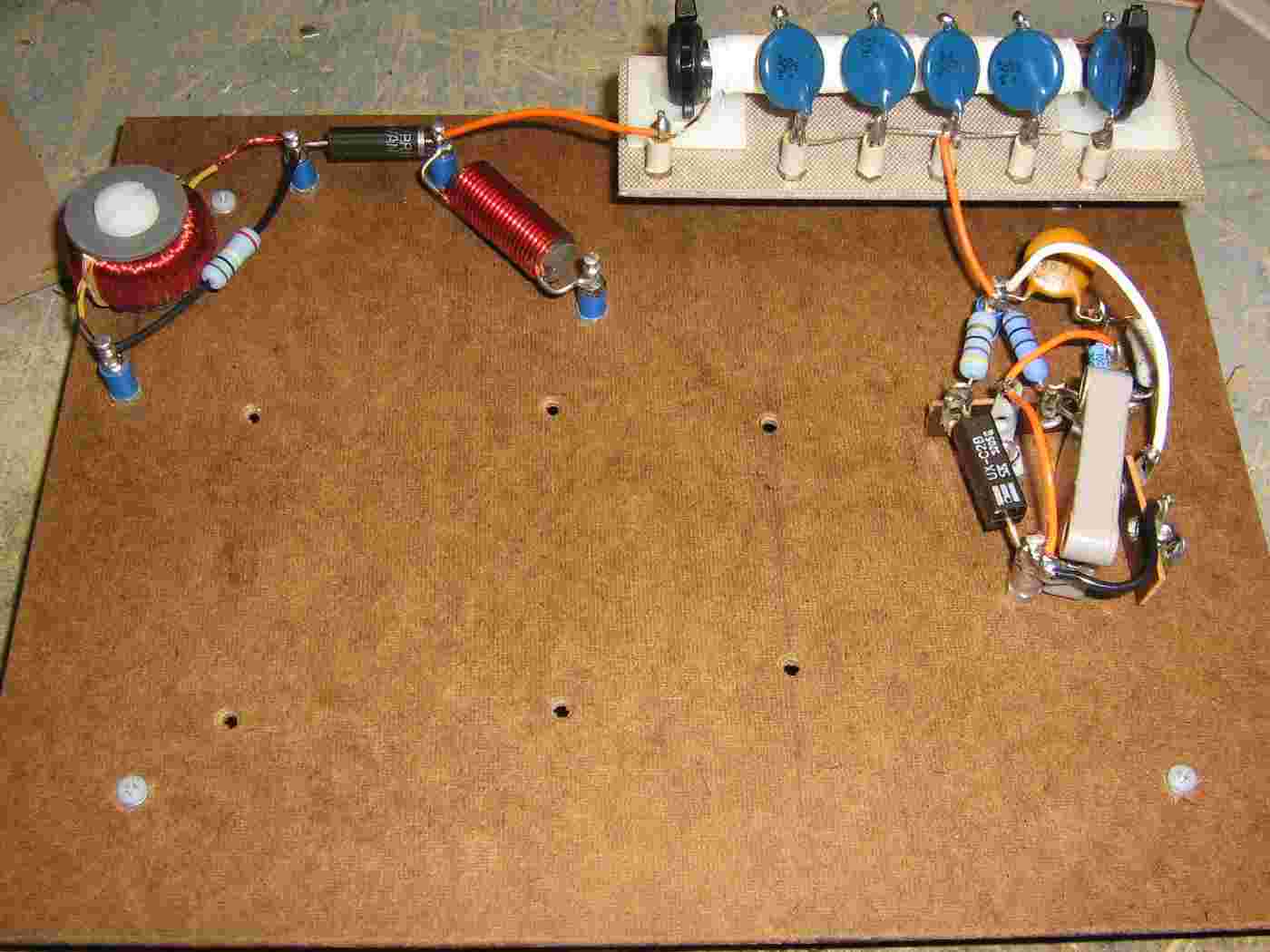
Overview of the input charging network, the PFN, and the output pulse circuit.
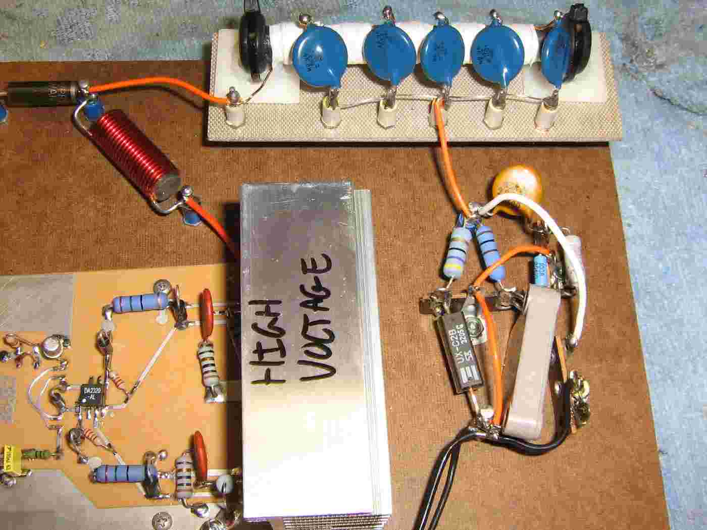
Close up picture of the output pulse circuit with the IGBT circuit (on the lower-left) now in place.
The series 100 ohm / 1,000 pF capacitor combination act as a surge de-spiker in case of an impedance mismatch with the magnetron. This can cause a large voltage "spike" from the pulse transformer.
The high-voltage diode is used as a "tail clipper" to clean up the shape of the final output voltage pulse. The series 47 ohm resistor is used to tame current spikes in the diode. The diode used here is a UX-C2B, or any voltage-doubler diode from an old microwave oven should work.
A series 220 pF high-voltage capacitor is used along with a 1,000 ohm resistor and 5.1 volt Zener diode to form an optional "pulse monitoring" circuit.
The final output pulse is via the WHITE wire on the left, with the BLACK wire being the common ground.
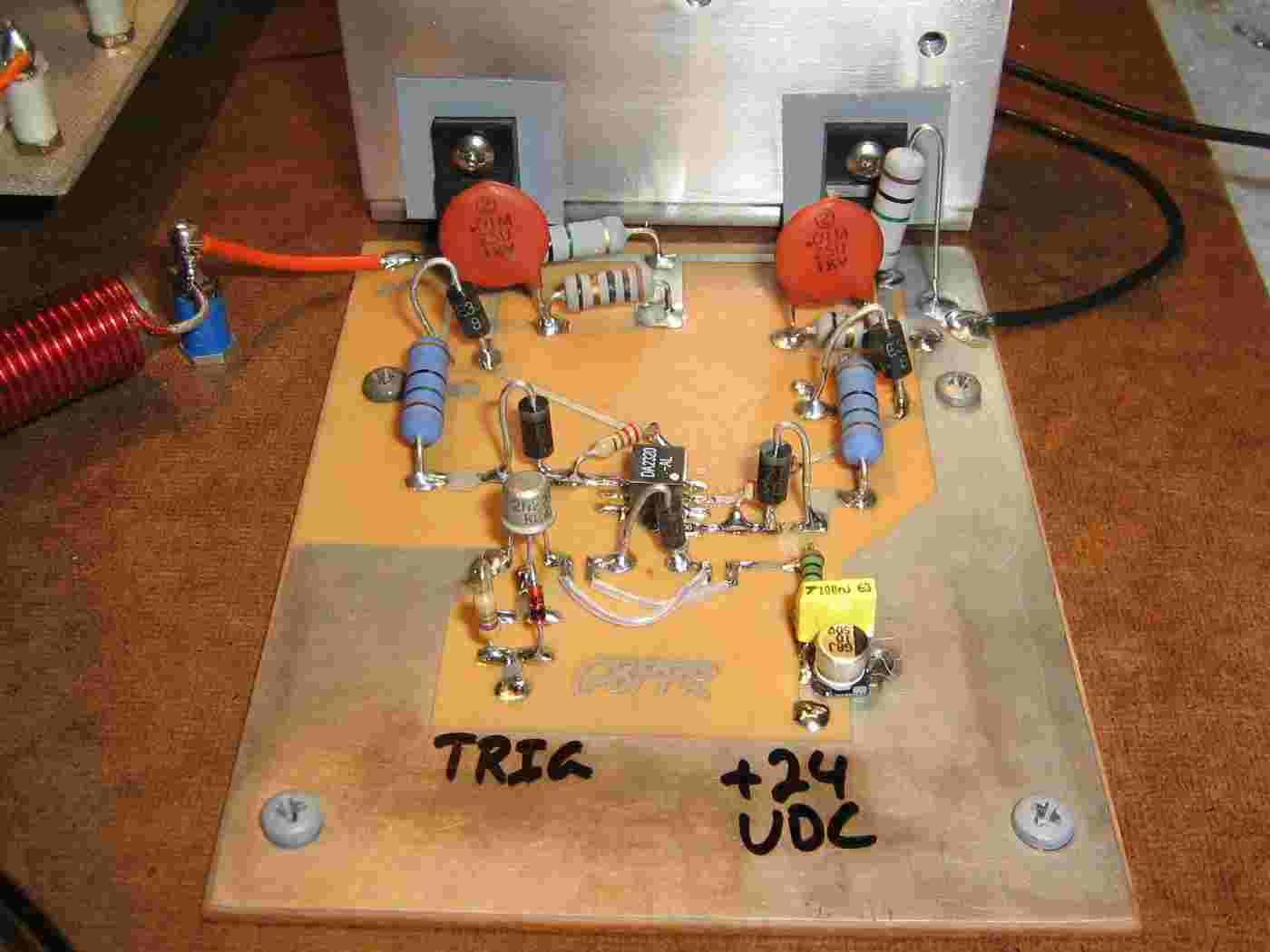
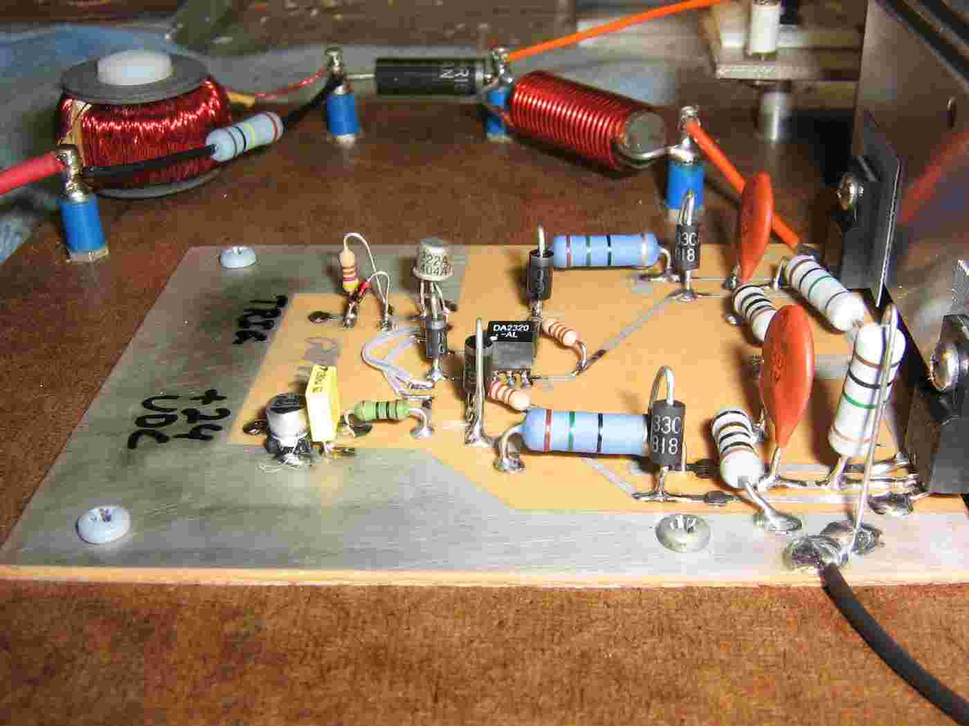
Overview of the two series ST Electronics STGF3NC120HD N-channel IGBTs and their gate-drive circuitry.
This is the section of the modulator which is still experimental.
The 2 kV DC input to the IGBTs is from the ORANGE wire on the left. The BLACK wire on the right is a common ground.
The +24 VDC for the gate-drive transformer's primary is on the lower-right. The trigger input to the 2N2222A is on the lower-left.
The little black box in the middle of the IGBTs is a Coilcraft DA2320 gate-drive transformer with a 1:1:1 turns ratio between the primary and secondary windings. This transformer is necessary to make sure the two IGBTs fire at the same time and provides proper high-voltage isolation. This transformer is a must. You can make your own using a ferrite core and some enameled wire. Google "gate-drive transformers" for alot more information on doing that.
The two 15 ohm (should be 10) resistors go to the gate's on the two IGBTs. A 33 volt TVS clamps any voltage spikes on the gate-drive signal to protect the IGBTs.
The capacitors and resistors across the two IGBTs help to equalize the high-voltage across the two IGBTs so one isn't "triggered" before the other.
The schematic and the above picture don't follow each other due to constant re-working.
Alternate view of the gate-drive circuits.
I originally had series diodes and loading resistors on the gate-drive transformer's output, but this seemed to distort the output signal.
You need a fast, clean square wave pulse-drive on the IGBT's gate for proper modulator operation, and so you can quickly re-charge the PFN after each pulse firing.

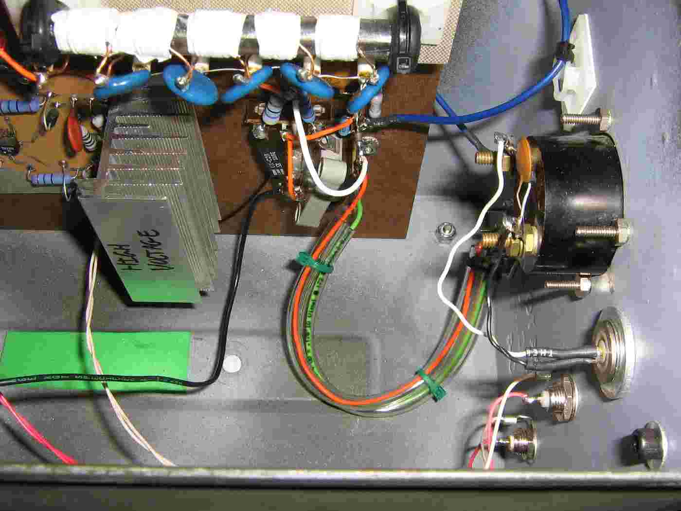
Overall view of the completed pulse modulator circuit.
The heatsink is isolated from ground, and probably overkill. The peak current through the IGBTs with this PFN and voltage is only around 10 Amps. The heatsink will help the pulse current handling of the IGBTs, but if not properly isolated, can arc from the high-voltage.
The IGBTs should have been mounted horizontally for a simpler layout design.
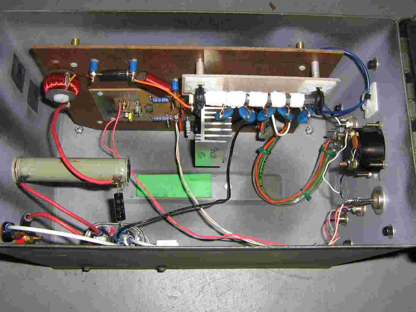
Overview of the pulse modulator's case.
Close up of the pulse output connection.
The output is via the ORANGE wire and goes to the center pin on a panel-mount SO-239 connector. The GREEN wire is a common ground. Vinyl tubing is used to increase the high-voltage isolation on the output wiring.
The pulse modulator's output will be sent to the magnetron's pulse transformer via some RG-62 (93 ohm) coax. This will be covered in an upcoming article.
The BLUE shielded wire is the output of the optional pulse monitor.
The high-voltage metering, the +24 VDC input, and the pulse trigger connections (from top-to-bottom) are via the BNC connectors on the lower-right.
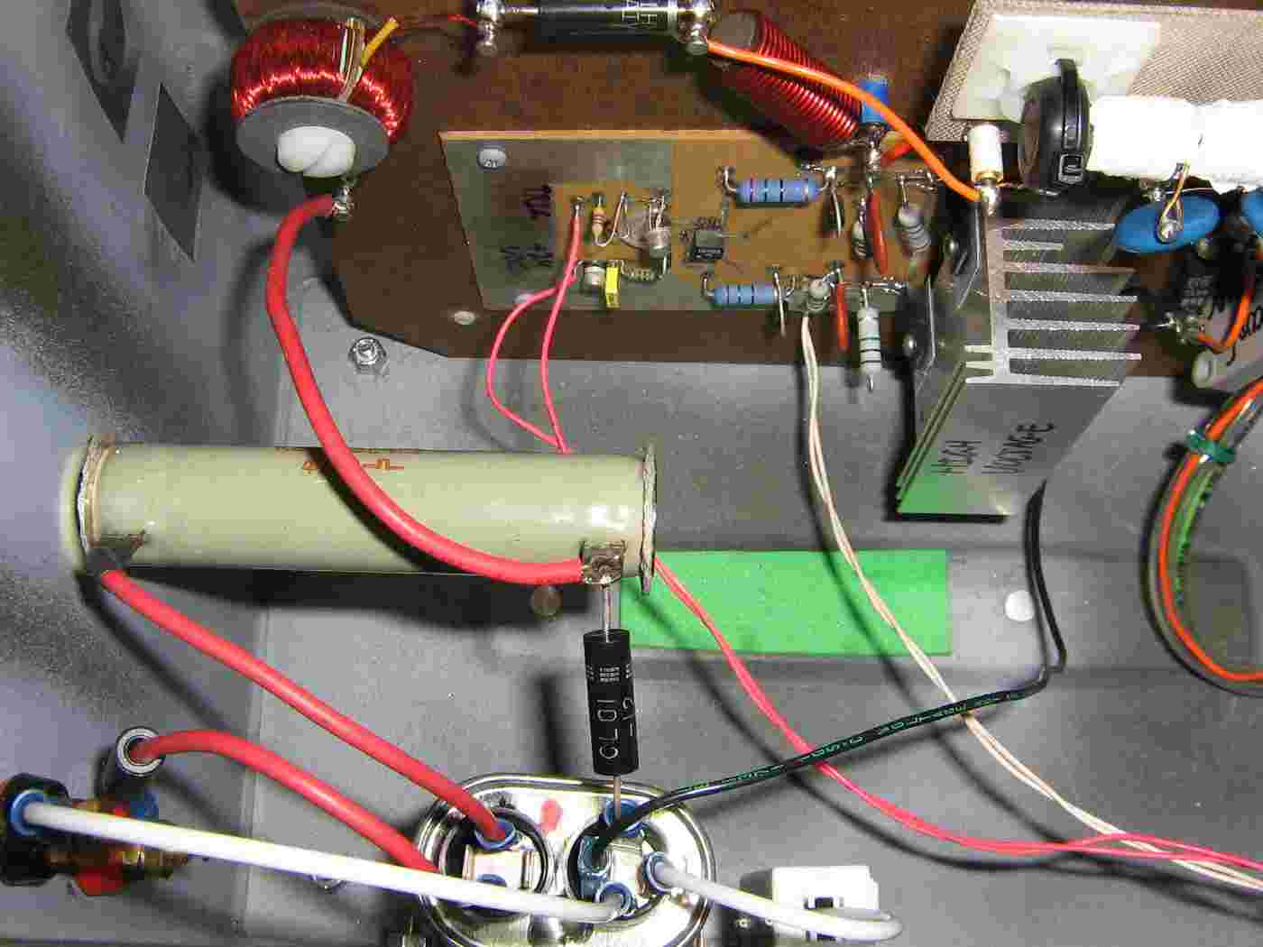
Close up of the high-voltage DC input network.
The positive for the 2 kV DC line is the via the RED banana jack.
The 1 µF microwave oven capacitor is on the bottom and has some ferrite beads on the positive and ground leads.
The big green cylinder is the series 47 ohm / 50 watt resistor.
The input protection diode is a CL01-12, or any voltage-doubler diode from an old microwave oven should work.
Be sure to follow proper high-voltage construction techniques when building this circuit.
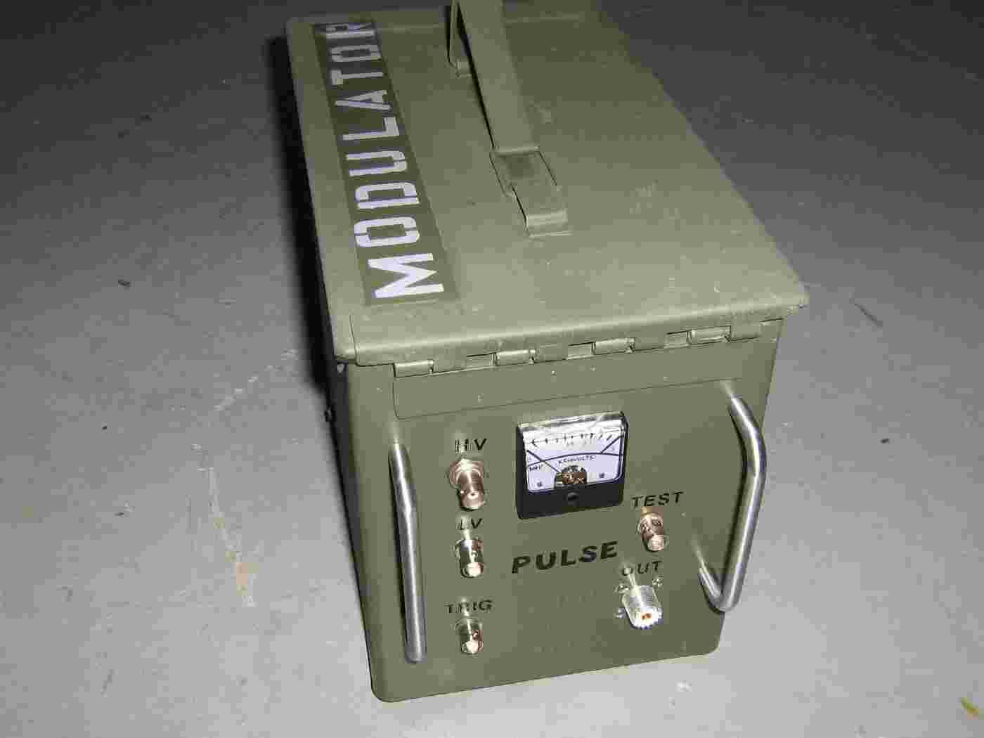
Finished outside case overview.
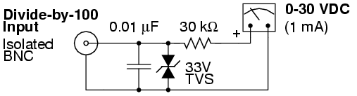
The high-voltage input monitoring meter is located in the top-center. Its "divide-by-100" input is via the female isolated BNC connector next to it marked "HV".
The Trigger Input is via the bottom female BNC connector on the lower left-side, marked "TRIG".
The +24 VDC Input is the female BNC connector above that, marked "LV".
The Pulse Output is via the SO-239 connector on the lower right-side, marked "OUT".
The optional Pulse Monitor output is via the female BNC connector above that, marked "TEST".
Final pulse modulator circuit testing can't really take place until the magnetron and its driving pulse transformer circuits are constructed.